![]()
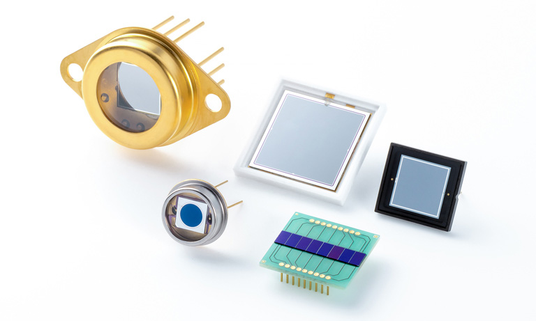
Products


We are actively taking measures to improve product quality levels.
Applications


Why Hamamatsu?
Resources


Support

Our company


Investors


United Kingdom (EN)
Select your region or country.

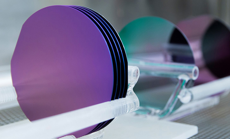
Semiconductor metrology and inspection
Meeting market demand for semiconductor wafers with high-radiance UV light sources
High production yields are critical to meeting today’s market demand for semiconductor wafers. Metrology and inspection are crucial steps in the long semiconductor manufacturing process to ensure the highest quality and yield.
Wafer metrology tools play a crucial role in the design and fabrication of high-performance integrated circuits (ICs) by aiding semiconductor manufacturers in minimizing defects and meeting increasing demands. Efficient characterization and measurement of thin films, line widths, pattern flaws, and other potential defects are essential for addressing issues swiftly, thereby reducing costly downtime. In semiconductor inspection, using higher radiance UV light sources becomes imperative to shorten inspection times and enhance accuracy in evaluating patterns and thin films on wafers.
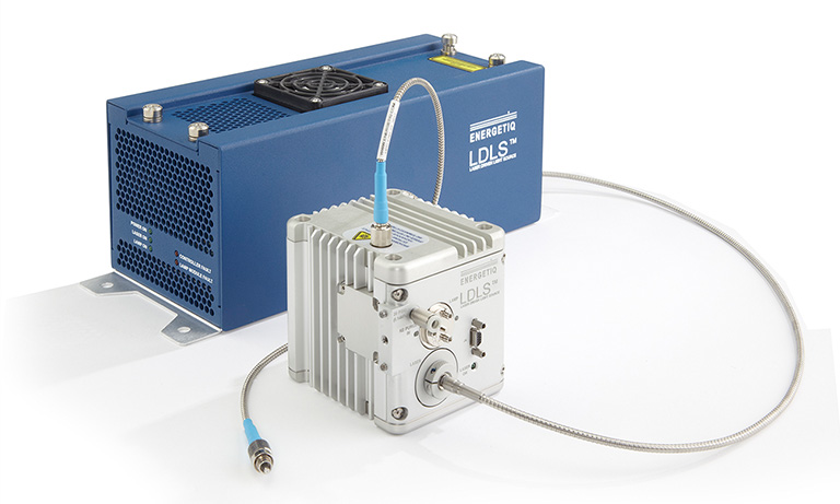
To respond to this demand, Energetiq Technology, a wholly owned subsidiary of Hamamatsu Photonics has combined its deep understanding of the plasma physics needed for high-brightness light generation with its long experience in building rugged products such as the Laser-Driven Light Source (LDLS®) and the Laser-Driven Tunable Light Source (LDTLS®).
High spectral radiance light sources
The broad wavelength, high spectral radiance light sources illuminate wafer anomalies with speed and accuracy. The unique principle of operation of the LDLS® with its small plasma size and high spatial stability enables high throughput measurements ideal for volume production environments.
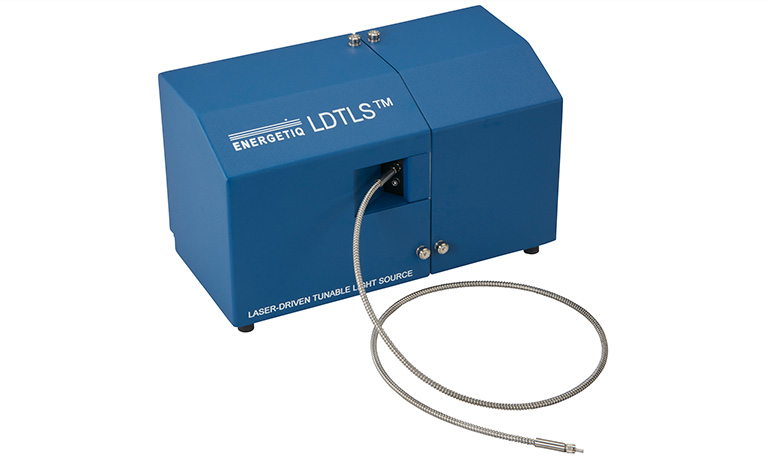
Its sister product, built on the same technology with the added tunable feature, the LDTLS® helps users break free from wavelength constraints for quick, repeatable, and precise measurements across a broader spectrum.
These solutions are optimal to meet the inspection needs because they provide excellent luminance over a broad spectral range along with a long service life.
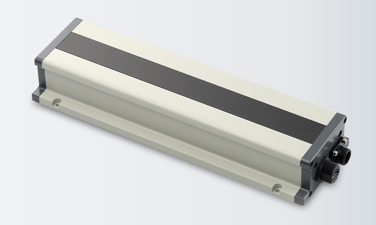
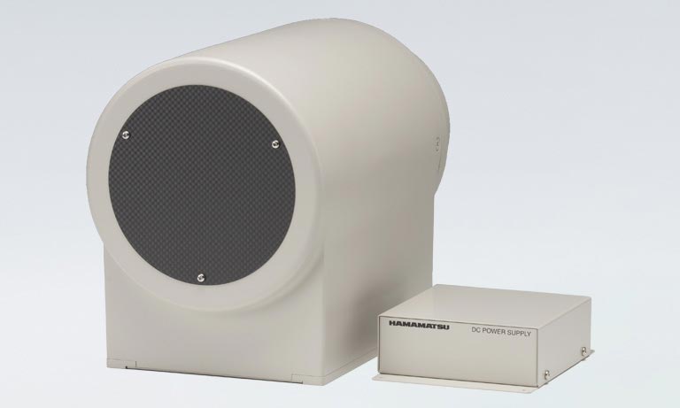
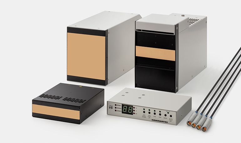
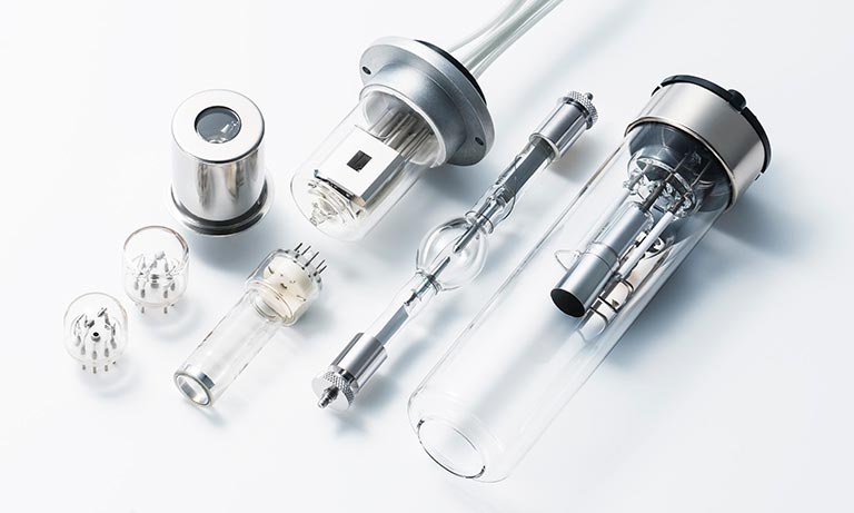
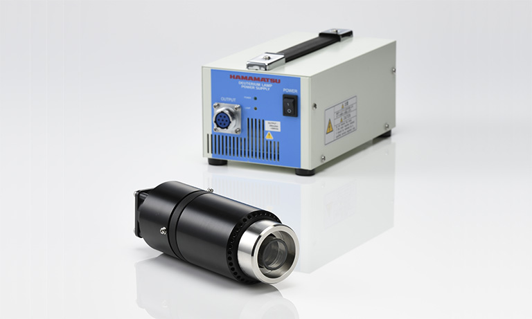
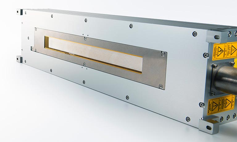
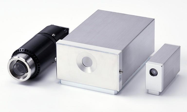
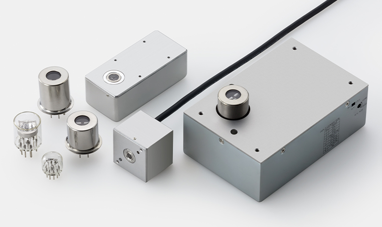
LDLS®
The LDLS® is one of the only light sources in the world that utilizes a focused laser beam to generate and maintain plasma between the discharge electrodes in the xenon gas-filled bulb. Learn more about this product by following this link: Laser-Driven Light Sources (LDLS®)
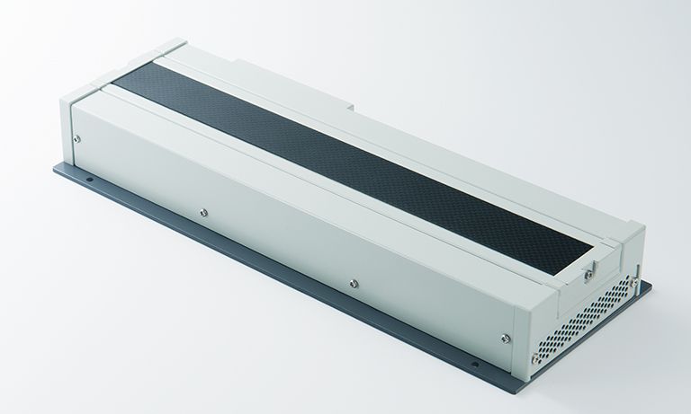
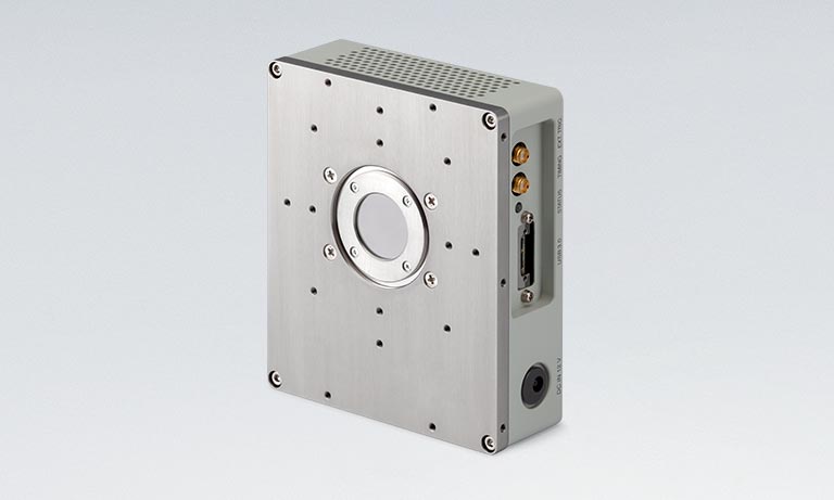
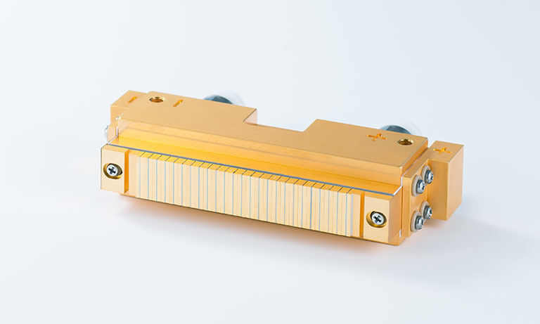
LDTLS®
Built around the LDLS® technology, the LDTLS® gives you access to a wide wavelength range of tunability, high spectral resolution, and an extremely long lifetime with the convenience of fiber-coupled output. The LDTLS® features a precision high-performance monochromator for accurate wavelength selection and repeatable light output.
Features:
- High spectral radiance for the highest output flux
- High output power
- Low noise, high stability
- 200 nm/second scan speed
- 10,000+ hours of operation
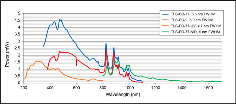
LDTLS® Typical in-band flux
LDTLS® product-range
| TLS-EQ-9 | TLS-EQ-77 | TLS-EQ-77-UV | TLS-EQ-77-NIR | |
|---|---|---|---|---|
| Wavelength Range | 380 nm - 1100 nm | 350 nm - 1100 nm | 200 nm - 770 nm | 800 nm - 1700 nm |
| Wavelength Accuracy | +/- 0.5 nm | +/- 0.5 nm | +/- 0.5 nm | +/- 0.5 nm |
| Scan Speed | <20 ms for a 2 ms step | <20 ms for a 2 ms step | <20 ms for a 2 ms step | <20 ms for a 2 ms step |
| Standard Optical Output | 1500 μm score diameter fibre optic cable | 1500 μm score diameter fibre optic cable | 1500 μm score diameter fibre optic cable | 1500 μm score diameter fibre optic cable |
| Numerical Aperture (NA) | 0.39 | 0.39 | 0.39 | 0.39 |
| Spectral Resolution (FWHM) | User selectable: 1.0 - 8.0 nm | 6.5 nm | 4.7 nm | 9 nm |
| Laser Class | Class 1 (IEC 60825: 2014) | Class 1 (IEC 60825: 2014) | Class 1 (IEC 60825: 2014) | Class 1 (IEC 60825: 2014) |
| Maximum In-Band Flux | 2.37 mW at 824 nm | 4.9 mW at 400 nm | 1.6 mW at 300 nm | 1.62 mW at 920 nm |
| Average In-Band Flux | ~1.20 mW | ~2.3 mW | ~1.1 mW (200 nm - 500 nm) | ~0.44 mW |
Resources
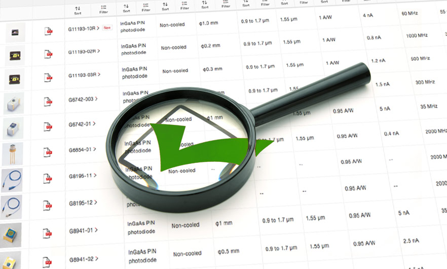
Read the extensive resources for additional information including application notes, articles, papers & posters, and more.
Recommended products
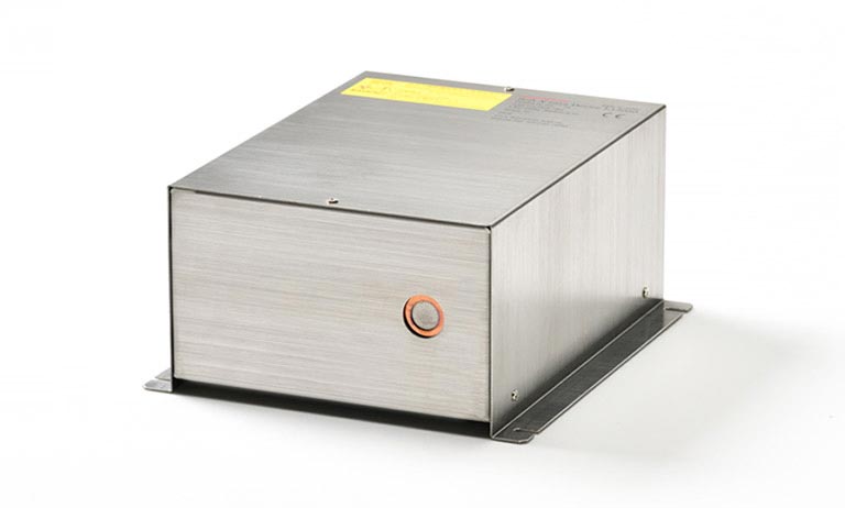
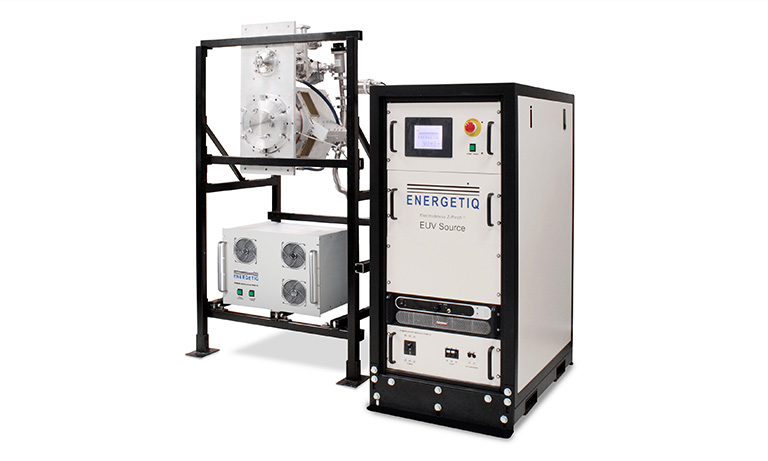
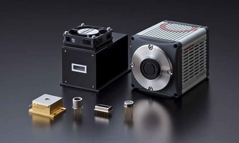
Besides the LDLS® and LDTLS®, Hamamatsu Photonics offers a full line-up of high-performance light sources including extreme ultraviolet (EUV) light sources and xenon lamps to respond to constantly changing needs in the semiconductor inspection equipment market.
Contact
If you are interested in this product, please contact us for the selection guide. The LDLS® and LDTLS® are products developed by Energetiq Technology inc. in the US, which is a subsidiary of Hamamatsu Photonics K.K.
- Confirmation
-
It looks like you're in the . If this is not your location, please select the correct region or country below.
You're headed to Hamamatsu Photonics website for GB (English). If you want to view an other country's site, the optimized information will be provided by selecting options below.
In order to use this website comfortably, we use cookies. For cookie details please see our cookie policy.
- Cookie Policy
-
This website or its third-party tools use cookies, which are necessary to its functioning and required to achieve the purposes illustrated in this cookie policy. By closing the cookie warning banner, scrolling the page, clicking a link or continuing to browse otherwise, you agree to the use of cookies.
Hamamatsu uses cookies in order to enhance your experience on our website and ensure that our website functions.
You can visit this page at any time to learn more about cookies, get the most up to date information on how we use cookies and manage your cookie settings. We will not use cookies for any purpose other than the ones stated, but please note that we reserve the right to update our cookies.
1. What are cookies?
For modern websites to work according to visitor’s expectations, they need to collect certain basic information about visitors. To do this, a site will create small text files which are placed on visitor’s devices (computer or mobile) - these files are known as cookies when you access a website. Cookies are used in order to make websites function and work efficiently. Cookies are uniquely assigned to each visitor and can only be read by a web server in the domain that issued the cookie to the visitor. Cookies cannot be used to run programs or deliver viruses to a visitor’s device.
Cookies do various jobs which make the visitor’s experience of the internet much smoother and more interactive. For instance, cookies are used to remember the visitor’s preferences on sites they visit often, to remember language preference and to help navigate between pages more efficiently. Much, though not all, of the data collected is anonymous, though some of it is designed to detect browsing patterns and approximate geographical location to improve the visitor experience.
Certain type of cookies may require the data subject’s consent before storing them on the computer.
2. What are the different types of cookies?
This website uses two types of cookies:
- First party cookies. For our website, the first party cookies are controlled and maintained by Hamamatsu. No other parties have access to these cookies.
- Third party cookies. These cookies are implemented by organizations outside Hamamatsu. We do not have access to the data in these cookies, but we use these cookies to improve the overall website experience.
3. How do we use cookies?
This website uses cookies for following purposes:
- Certain cookies are necessary for our website to function. These are strictly necessary cookies and are required to enable website access, support navigation or provide relevant content. These cookies direct you to the correct region or country, and support security and ecommerce. Strictly necessary cookies also enforce your privacy preferences. Without these strictly necessary cookies, much of our website will not function.
- Analytics cookies are used to track website usage. This data enables us to improve our website usability, performance and website administration. In our analytics cookies, we do not store any personal identifying information.
- Functionality cookies. These are used to recognize you when you return to our website. This enables us to personalize our content for you, greet you by name and remember your preferences (for example, your choice of language or region).
- These cookies record your visit to our website, the pages you have visited and the links you have followed. We will use this information to make our website and the advertising displayed on it more relevant to your interests. We may also share this information with third parties for this purpose.
Cookies help us help you. Through the use of cookies, we learn what is important to our visitors and we develop and enhance website content and functionality to support your experience. Much of our website can be accessed if cookies are disabled, however certain website functions may not work. And, we believe your current and future visits will be enhanced if cookies are enabled.
4. Which cookies do we use?
There are two ways to manage cookie preferences.
- You can set your cookie preferences on your device or in your browser.
- You can set your cookie preferences at the website level.
If you don’t want to receive cookies, you can modify your browser so that it notifies you when cookies are sent to it or you can refuse cookies altogether. You can also delete cookies that have already been set.
If you wish to restrict or block web browser cookies which are set on your device then you can do this through your browser settings; the Help function within your browser should tell you how. Alternatively, you may wish to visit www.aboutcookies.org, which contains comprehensive information on how to do this on a wide variety of desktop browsers.
5. What are Internet tags and how do we use them with cookies?
Occasionally, we may use internet tags (also known as action tags, single-pixel GIFs, clear GIFs, invisible GIFs and 1-by-1 GIFs) at this site and may deploy these tags/cookies through a third-party advertising partner or a web analytical service partner which may be located and store the respective information (including your IP-address) in a foreign country. These tags/cookies are placed on both online advertisements that bring users to this site and on different pages of this site. We use this technology to measure the visitors' responses to our sites and the effectiveness of our advertising campaigns (including how many times a page is opened and which information is consulted) as well as to evaluate your use of this website. The third-party partner or the web analytical service partner may be able to collect data about visitors to our and other sites because of these internet tags/cookies, may compose reports regarding the website’s activity for us and may provide further services which are related to the use of the website and the internet. They may provide such information to other parties if there is a legal requirement that they do so, or if they hire the other parties to process information on their behalf.
If you would like more information about web tags and cookies associated with on-line advertising or to opt-out of third-party collection of this information, please visit the Network Advertising Initiative website http://www.networkadvertising.org.
6. Analytics and Advertisement Cookies
We use third-party cookies (such as Google Analytics) to track visitors on our website, to get reports about how visitors use the website and to inform, optimize and serve ads based on someone's past visits to our website.
You may opt-out of Google Analytics cookies by the websites provided by Google:
https://tools.google.com/dlpage/gaoptout?hl=en
As provided in this Privacy Policy (Article 5), you can learn more about opt-out cookies by the website provided by Network Advertising Initiative:
http://www.networkadvertising.org
We inform you that in such case you will not be able to wholly use all functions of our website.
Close