![]()
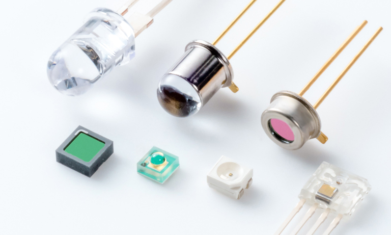
Products


We are actively taking measures to improve product quality levels.
Applications


Why Hamamatsu?
Support


Our company
Investors


Japan (EN)
Select your region or country.

History
Took up further challenges in very low-light-level measurement and single photon detection.
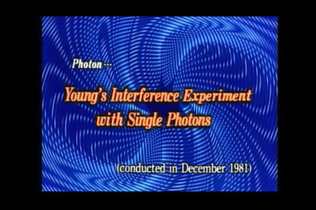
Succeeded in conducting Young's interference experiment with single photons.
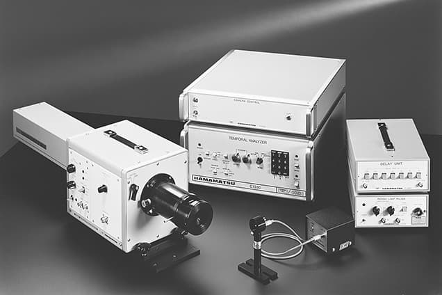
Using the PIAS (Photon-counting Image Acquisition System), we conducted Young's double-slit interference experiment in the single photon counting region. This demonstrated that an interference pattern appeared by detecting individual photons one by one and then integrating them to create an image. The experimental results indicated that one photon passed through the double slit at the same time (wave interference) and then created one bright spot on the detector (particle’s photoelectric effect). Integrating each bright spot resulted in an image of interference fringes which clearly demonstrated dual properties of light (light is both a wave and a particle). The PIAS imaging system used for this experiment was named one of the “10 Great New Products 1984” by Nikkan Kogyo Shimbun in Japan and also earned an R&D Award from R&D Magazine in the USA. This definitely proved that our low-light-level measurement technology was highly appreciated both domestically and abroad.
Photo: Young’s interference experiment with single photons
Timeline
Pursuing the path of light
First starting from the founding of Tokai Electronics Laboratory in 1948, Hamamatsu TV Co., Ltd. was then established in 1953 followed by a company name change to Hamamatsu Photonics K.K. in 1983. All through this period and up to the present day, we here at Hamamatsu Photonics have been continually pursuing technologies involving “light” in all its aspects. Take a look along with us at the history of our company constantly pursuing the path of light since our founding.
Timeline
1948-1950s 

Founding of the firm: Starting to challenge the possibilities of light
1948
Heihachiro Horiuchi founded Tokai Electronics Laboratory.
Project was launched amidst the ruins after the war with the dream of developing photoelectric devices.
Heihachiro Horiuchi founded Tokai Electronics Laboratory.
Project was launched amidst the ruins after the war with the dream of developing photoelectric devices.
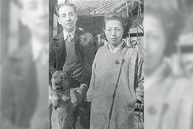
Being fascinated by the wonder of light since the elementary school days, our founding president Heihachiro Horiuchi studied Electrical Engineering at Hamamatsu Industrial High School (now the Faculty of Engineering of Shizuoka University) as a student of Kenjiro Takayanagi who was one of the world’s pioneers of television technology research, and was greatly inspired by “Takayanagi-ism” after receiving his guidance and instruction. During the World War 2, Heihachiro Horiuchi worked on developing and manufacturing night-vision tubes in Tokyo and then in Yamagata in the northern region of Japan where the factory was evacuated due to bombing. However, when the war ended he had to completely restart his career. He returned to Hamamatsu in the post-war chaos and made a decision to utilize the photoelectric technology he had learned before and during the war. In 1948, he bought a factory site at 456 Ebitsuka-cho, Hamamatsu City, and established Tokai Electronics Laboratory.
Photo: Heihachiro Horiuchi and his wife Hiroko, with their dog Mac
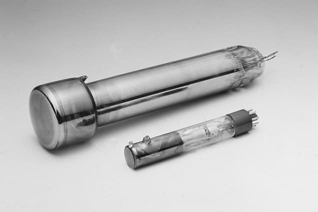
1951
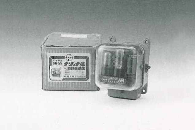
Developed the PV26 phototubes that were used for automatic on/off street light switching.
1953
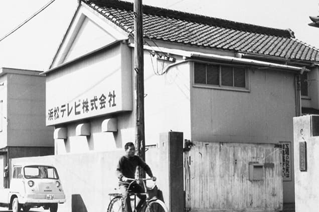
Established Hamamatsu TV Co., Ltd. with the dream of linking optical technology with industry.
Read full storyEstablished Hamamatsu TV Co., Ltd. with the dream of linking optical technology with industry.
Horiuchi decided to pursue the “path of light” by providing society with a means or namely products that would make effective use of light and he worked on developing photoelectric devices. In early 1951, Horiuchi’s efforts began to show signs of success as a promising inquiry came in for phototubes later called the PV29 and PV26 that he first worked on. At that point in time, Horiuchi was planning to dissolve Tokai Electronics Laboratory into another organization, and so he convinced Teruo Hiruma and Norio Hanyu, who he knew through his elder brother Yuji Takahashi (then Professor at Hamamatsu Industrial High School), to participate in his plan to establish a new company. This gave rise to the founding of Hamamatsu TV Co., Ltd.
Photo: Ebitsuka factory at that time
Started production of G5E phototubes for fax transmissions.
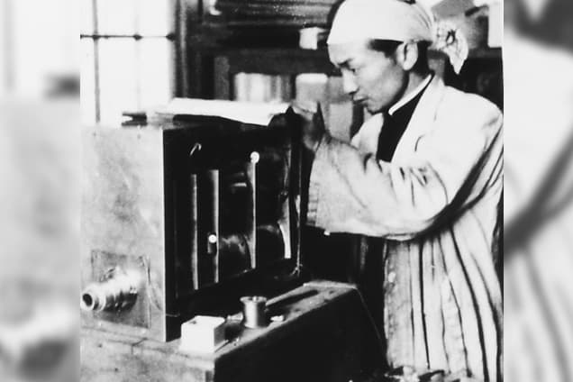
Developed an underwater camera as our first video camera product.
Started finding applications in scientific and industrial fields.
Developed an underwater camera as our first video camera product.
Started finding applications in scientific and industrial fields.
We became involved in television applications in the fields of science and industry when we were asked by Professor Nobuyuki Kawamoto of Mie University to make an underwater camera for observing fish reefs. That was our first attempt to make a television camera. Preliminary experiments were successful and reported in newspaper, but the actual experiment with the camera loaded on the experimental ship did not succeed unfortunately. Nevertheless, this first attempt to make a television camera was a significant step as our first field experiment.
Photo: Assembly and adjustment of underwater camera
1956
Placed selenium photocathode vidicons on the market.
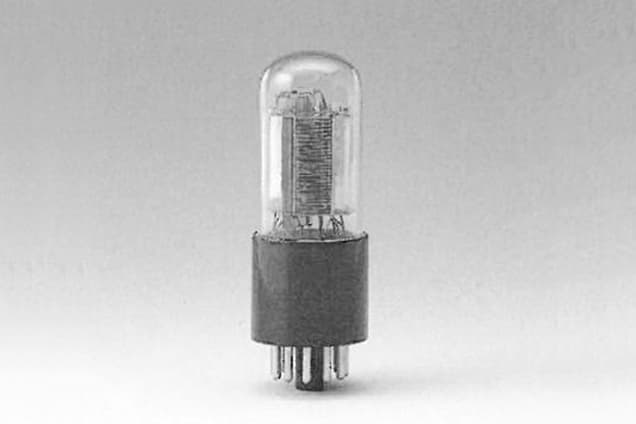
1958
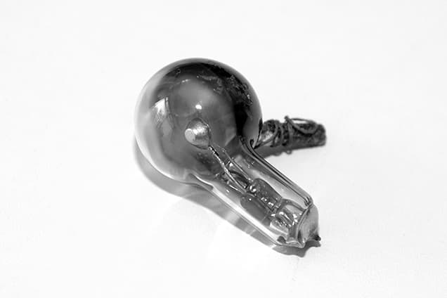
Developed CdS cells that were our first semiconductor products.
Our first mass-production line started up.
Developed CdS cells that were our first semiconductor products.
Our first mass-production line started up.
Up until that point, Hamamatsu TV had always been involved in electron tube products such as phototubes. Our first foray into semiconductor products was the CdS cell. After a hard struggle and repeated trials and errors, an employee succeeded in developing the product . One day at the end of 1958, an order came in for 1,000 CdS cells per month for use in adjusting the brightness of television cathode ray tubes. As a company that had up until that time been producing multiple products in small lots, it was our first experience with mass production, and we had to mobilize all of our employees on the production side to get the order filled. The development of the CdS cell ended up bringing about many positive outcomes, among them an accumulation of semiconductor technology and a new sense of unity in-house, after all of the employees had worked together day and night on the production effort.
Photo: Our first CdS Cell: the P101
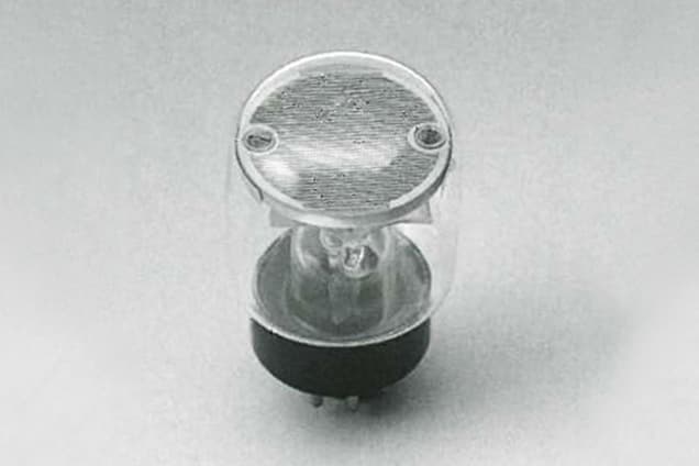
1959
Succeeded in developing photomultiplier tubes that are still our main products.
Read full storySucceeded in developing photomultiplier tubes that are still our main products.
Among various types of photodetectors, photomultiplier tubes offer superior features such as extremely high sensitivity and fast time response. Around 1955, chemical analysis instruments using photomultiplier tubes began to be manufactured and demand for them also increased in Japan. However, most of such equipment was imported from overseas at that time.Around that time, one of our customers said to us, "If Hamamatsu TV could produce photomultiplier tubes, we would call you the 'king' of the industry." That made our engineers realize the necessity for development of these tubes, and provided the motivation for them to undertake the project. The photomultiplier tube that they developed through many trials and tribulations was far superior to those of other companies, and that product was what gave us a solid footing as an opto-technology company.
Photo: Our first photomultiplier tube: the 931A
1960s
Business expansion and development: Taking up new challenges in unknown fields
1963
Placed infrared video cameras on the market.
1964
Opend our Ichino Factory.
1966
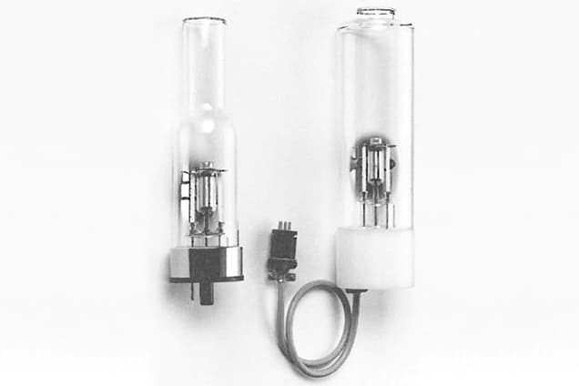
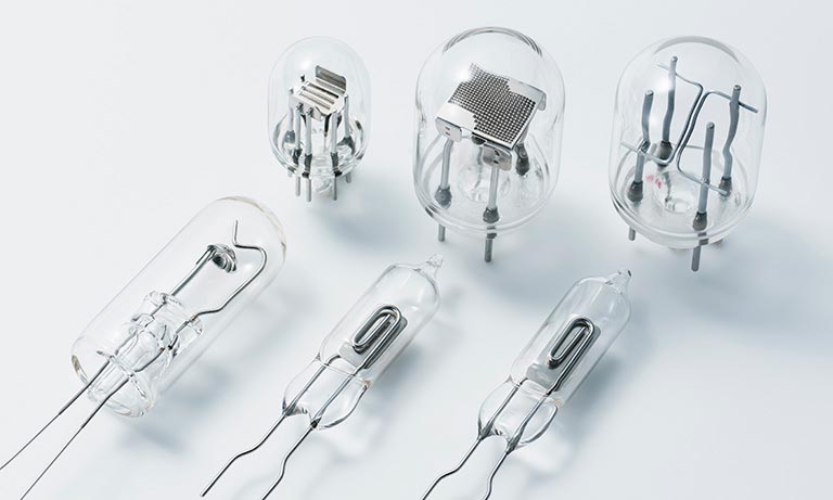
Experimental production of hollow cathode lamps and deuterium lamps began.
Opened our New York office.
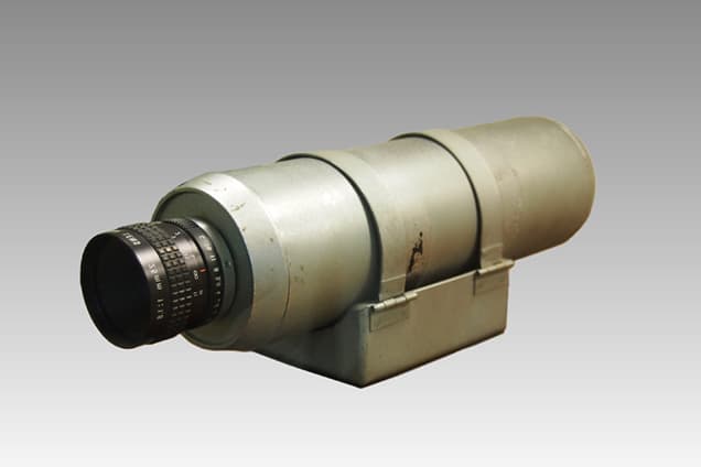
1967
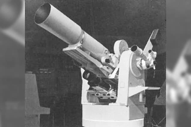
Succeeded in developing an automatic rocket tracking system called the X-Y Tracker.
Started to take part in space development projects.
Succeeded in developing rocket automatic tracking device
Participation in the space development project began.
We spent two years developing automatic rocket tracking system (the X-Y tracker), something that was requested by Professor Tsuneyoshi Uemura of Tokyo University, and after many hardships we succeeded in creating a prototype. This X-Y tracker was able to flawlessly track the rocket immediately after launch, and observers visiting from America praised it highly, saying that it was the most advanced device of anything that they had seen at the Uchinoura test facility. At that time, even NASA was using photographic strip film for orbital tracking of rockets, and the X-Y tracker was truly an epochal device. It provided the opportunity for us to take part in space development projects such as cameras for observing the aurora borealis and cameras for the "Suisei", the probe tracking Halley's comet.
Photo: Automatic rocket tracking system called the X-Y Tracker
1969
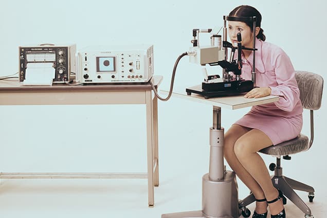
Expanded into medical fields.
Developed an eye pupil area measurement system using a video camera.
Expanded into medical fields.
Developed an eye pupil area measurement system using a video camera.
Tetsu Ishikawa, a lecturer at the Tokyo University Faculty of Medicine, thought that if a device were developed that made it possible to accurately measure pupillary responses (changes in the surface area of the iris) closely related to autonomous nervous system functions, it would be the first such device in the world to be able to do so, and he came to us to see if we could develop it. The development of this "Iriscoder" not only required that we focus everything on improving the product precision, as we had in the past, but also required that we take on a field that was completely unknown to us. That was the field of medical equipment manufacturing, which included camera performance, the convenience of use for physicians, taking the psychological state of the subject into consideration, and other elements with which we were unfamiliar. This device was used to study pupillary responses (adaptation of the eye to darkness and brightness) when entering and driving through tunnels, and the results of those experiments are still at work today in expressway tunnel illumination.
Photo:Iris testing using the Iriscoder
Established an affiliated company in the USA
1970s
Preparation for the big leap: Laying the cornerstone for solid-state products and system products.
1972
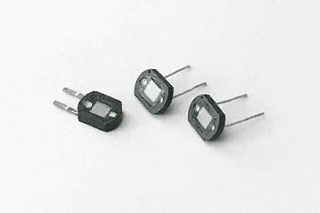
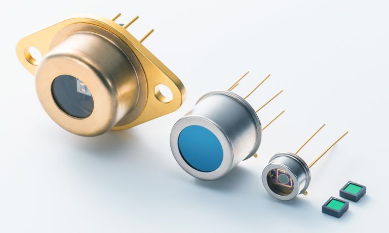
Developed silicon photodiodes based on the technical expertise we had accumulated through the development and manufacture of electron tubes.
Read full storyDeveloped silicon photodiodes based on the technical expertise we had accumulated through the development and manufacture of electron tubes.
Around that time, the camera maker to whom we were supplying CdS cells asked us to develop a silicon photodiode for use with cameras, saying that, as semiconductor components, these photodiodes offered better measurement accuracy and response characteristics than CdS cells. Silicon photodiodes were viewed as very promising at the time as sensors for camera exposure meters and measuring instruments. We got off to a late start in that field, but we drew on the knowhow and the sales channels that we had built up through our electron tube development and manufacturing, and silicon photodiodes later grew to be one of the main products of our Solid State Division.
Photo: Silicon photodiodes
1973
Opened our Toyooka Factory.
Established a joint venture company in West Germany (now Germany).
1977
Placed streak camera systems on the market.
Opening up new borders through connections with computers.
Developed vidicon camera for computers.
Opening up new borders through connections with computers.
Developed vidicon camera for computers.
In 1971, microcomputers appeared on the market and their use spread rapidly. We were quick to open up new frontiers in computer-compatible video cameras. The model C1000 (vidicon camera for computers) was an innovative high-precision video camera with the basic performance and functions needed for image processing and measurement. This was quite different from other conventional video cameras that were designed just for “viewing” tasks such as for monitoring and surveillance. The C1000 enabled sophisticated image processing using a computer and its applications were extended to various fields. This combination of video camera and computer is still a feature of our current system products.
Photo: The C1000 vidicon camera for computers
1978
A space-borne TV camera we developed helped succeed in capturing aurora images from outer space for the first time in the world.
Read full storyA space-borne TV camera we developed helped succeed in capturing aurora images from outer space for the first time in the world.
“I’d like to observe auroras from outer space by mounting a TV camera on an artificial satellite.” We received a request to develop a satellite-borne TV camera from Prof. Takao Tohmatsu, an authority on geophysics of the Geophysics Research Laboratory, University of Tokyo. In a limited time, we worked to develop a vacuum UV image storage tube and a TV camera that would be able to operate reliably for a period of one year under harsh conditions in space such as a vacuum, extremely cold or hot temperatures, and exposure to radiation, as well as having the high durability needed against vibration and shocks applied during the satellite launch. In 1978, the Japanese scientific satellite EXOS-A (later named “Kyokko”) equipped with our special TV camera was launched. After 20 days, when the satellite had traveled around the earth 214 times, it succeeded in capturing 8 beautiful images of an aurora among the 20 images that were taken at that time. This was the first success in the world in capturing aurora images from outer space, and made our company name well-known worldwide in the field of space development.
Photo: Satellite-borne TV camera
25th anniversary of company foundation. Teruo Hiruma became the company's president.
1980s
The age of photonics: Changing from Hamamatsu TV Co., Ltd. to Hamamatsu Photonics K.K.
1980
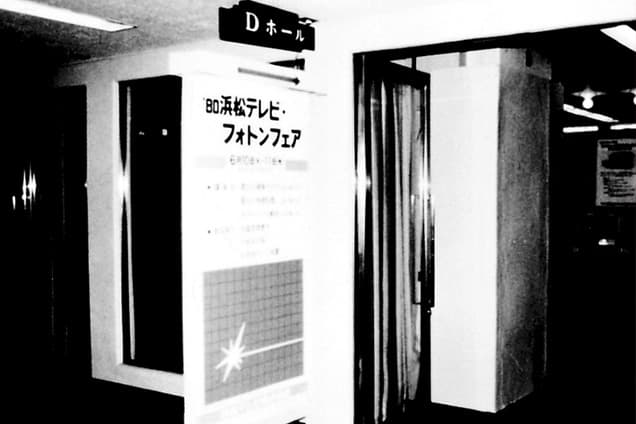
Our first private exhibition called the Photon Fair was held to introduce and demonstrate our wide-ranging photonics technology and products.
Read full storyOur first private exhibition called the Photon Fair was held to introduce and demonstrate our wide-ranging photonics technology and products.
Having had a good response from customers visiting our "Hamamatsu General Exhibition Osaka" held in 1979 to commemorate the opening of our Osaka sales office, we also held our first overall exhibition called the Photon Fair the next year 1980 in Osaka and Tokyo. The exhibition name Photon Fair was derived from the elementary particle called a photon used in our business slogan “Photon is our business” so as to let more people become familiar with the exhibition. Besides just exhibiting a full range of our products, we also introduced new technologies and made efforts to provide technical consultations, lectures and workshops, so that we could propagate our business philosophy and attitude by way of the Photon Fair. Even now, the Photon Fair is held regularly as an effective place for meeting and talking with customers to exchange ideas and information.
Photo: Entrance to the exhibition hall where the first Photon Fair was held
1982
Decided to reorganize the company into business divisions for greater flexibility in meeting business needs of the changing times.
Read full storyDecided to reorganize the company into business divisions for greater flexibility in meeting business needs of the changing times.
Up to that time, our production department had been managed and controlled as one basic unit. However, since the company’s scale had expanded and the number of product types had increased, we reorganized the company into business divisions to quickly and accurately respond to the changing times and offer more flexible business operations. The company was divided into 3 business divisions: Electron Tube Division, Solid State Division, and Systems Division. The main office and factories of each division had been gathered in an area different from each other, so they have been located there up to today.
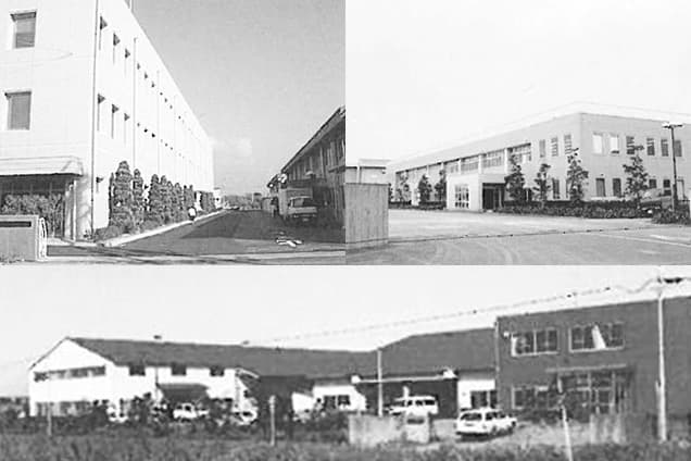
Photo: Main office and factories of each division at that time the company was reorganized
Took up further challenges in very low-light-level measurement and single photon detection. Succeeded in conducting Young's interference experiment with single photons.
Read full story1983
Changed our company name to Hamamatsu Photonics K.K.
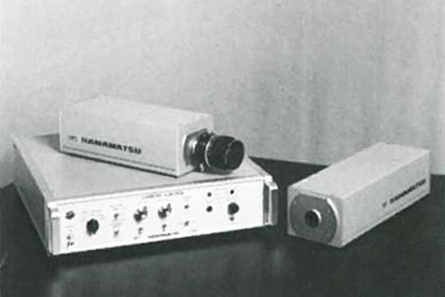
Placed Photonic microscope systems (video camera systems for microscopes) on the market.
1984
Placed the PIAS (Photon-counting Image Acquisition System) on the market.
Officially registered on over-the-counter market of Japan Securities Dealers Association.
Placed xenon lamps on the market.
1985
Opened our headquarters business office in Sunayama-cho, Hamamatsu City.
Established an affiliated company in France.
Placed high power pulsed laser diodes on the market.
1988
Japanese Prince Akihito (now the emperor emeritus) visited our Toyooka Factory.
Established affiliated companies in the UK and Sweden and a joint venture company (manufacturing subsidiary company) in China.
1990s
Beginning of new explorations: Stepping forward to contribute to better human life
1990
Opened our Hamamatsu Photonics Central Research Laboratory.
1991
Established an affiliated company in Italy.
1994
Opened our Miyakoda Factory.
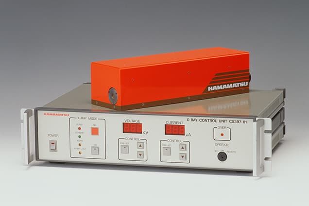
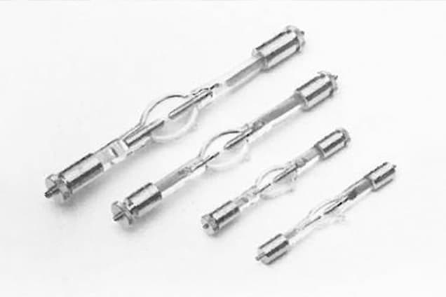
Placed micro focus X-ray sources on the market.
1996
Company's stock registered on the second section of the Tokyo Stock Exchange.
1998
Company's stock registered on the first section of the Tokyo Stock Exchange.
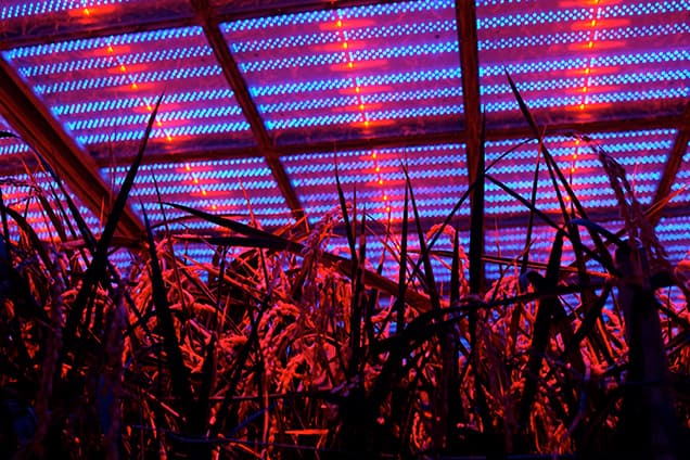
Succeeded for the first time in the world in artificial indoor cultivation of rice plants using semiconductor lasers.
Read full storySucceeded for the first time in the world in artificial indoor cultivation of rice plants using semiconductor lasers.
This plant factory succeeded in artificially cultivating rice plants in an indoor farm, for the first time in the world using high-power semiconductor lasers instead of sunlight. This experiment relied on semiconductor lasers that were fabricated by applying our technology developed for laser fusion research. Those semiconductor lasers were designed to emit light at 680 nm where the chloroplasts in rice leaves photosynthesize most vigorously. Compared to conventional cultivation methods used in plant factories, this new method applying semiconductor lasers drastically cuts the power cost and shortens the cultivation period, offering the possibility of eliminating global food shortage in the future.
Photo: Plant factory
2000s
Pioneering for the next generation: Aiming at creating new industries
2002
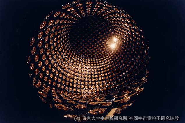
Nobel Prize in physics awarded to Masatoshi Koshiba, professor emeritus of University of Tokyo, for research conducted at Kamiokande where a large number of our photomultiplier tubes were installed.
Read full storyNobel Prize in physics awarded to Masatoshi Koshiba, professor emeritus of University of Tokyo, for research conducted at Kamiokande where a large number of our photomultiplier tubes were installed.
Photo: Inside of Kamiokande
2003
The building of a clinical facility for the Hamamatsu Medical Imaging Center run by the Hamamatsu Medical Photonics Foundation was completed to facilitate the early detection of cancer and dementia.
2005
Opened the Graduate School for the Creation of New Photonics Industries with the goal of creating new photonics industries.
Read full storyOpened the Graduate School for the Creation of New Photonics Industries with the goal of creating new photonics industries.
As we move into the 21st century, remarkable globalization is taking place throughout the world in both industrial and economic sectors. In Japan, which has built the foundation for an economic empire by taking academic learning and technologies introduced from foreign countries and further developing and expanding applications for those technologies, we're now finding that we ourselves need to create new industries, and in turn new cultures, which we can then send out into the rest of the world. The Graduate School for the Creation of New Photonics Industries was established by Hamamatsu Photonics and other enterprises for the purpose of cultivating human resources capable of launching new industries that will focus on light and its infinite possibilities. Put differently, the founding of new industries itself is the foremost objective of education at the University.
Photo: The Graduate School For The Creation Of New Photonics Industries
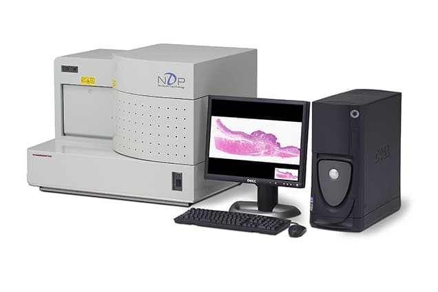
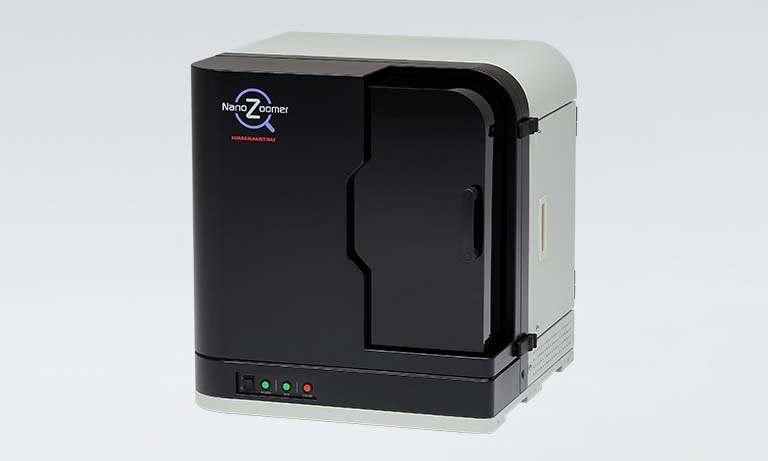
Placed NanoZoomer digital slide scanners on the market.
2009
Akira Hiruma took office as president and CEO.
2010s
From Hamamatsu to the world: Making further progress toward global expansion
2010
Established a European headquarters to streamline business activities among sales subsidiaries in Europe.
2011
Established an affiliated company as sales subsidiary in China.
2013
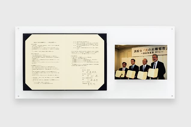
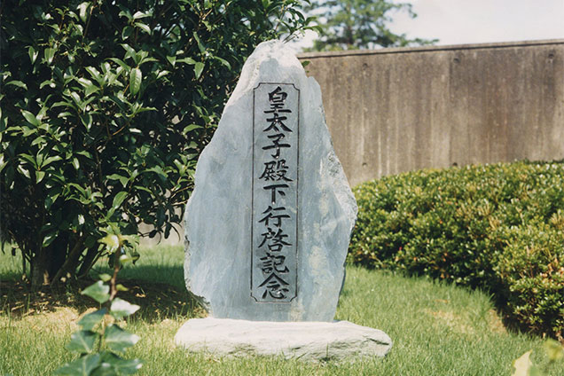
Signed the "Photonics Declaration in Hamamatsu 2013 - for establishing Hamamatsu as a Preeminent Photonics City" along with 3 nearby universities.
Read full storySigned the "Photonics Declaration in Hamamatsu 2013 - for establishing Hamamatsu as a Preeminent Photonics City" along with 3 nearby universities.
Photo: Written declaration
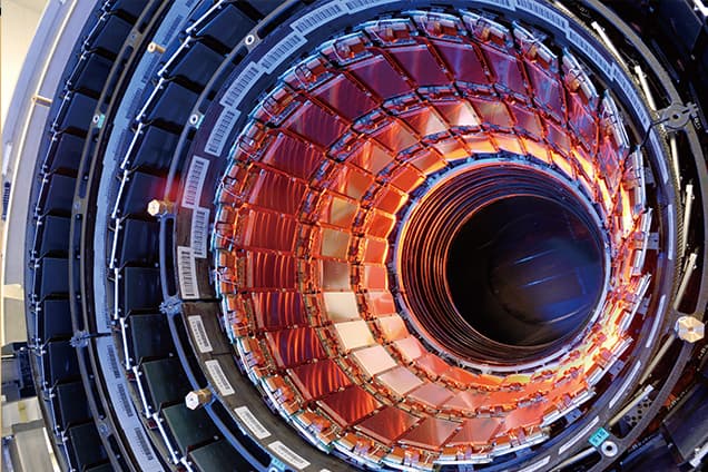
Our SSD, APD and photomultiplier tubes contributed to detection of Higgs bosons.
Nobel Prize in physics awarded to Professors emeritus Francois Englert and Peter W. Higgs for the detection of Higgs bosons.
Our SSD, APD and photomultiplier tubes contributed to detection of Higgs bosons.
Nobel Prize in physics awarded to Professors emeritus Francois Englert and Peter W. Higgs for the detection of Higgs bosons.
Photo: SSD (silicon strip detectors) installed inside the Large Hadron Collider at CERN
2014
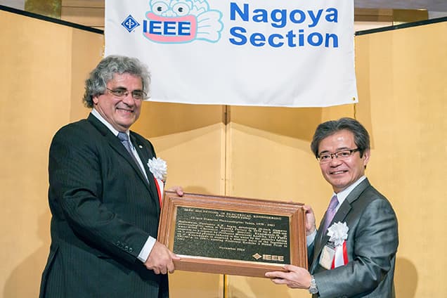
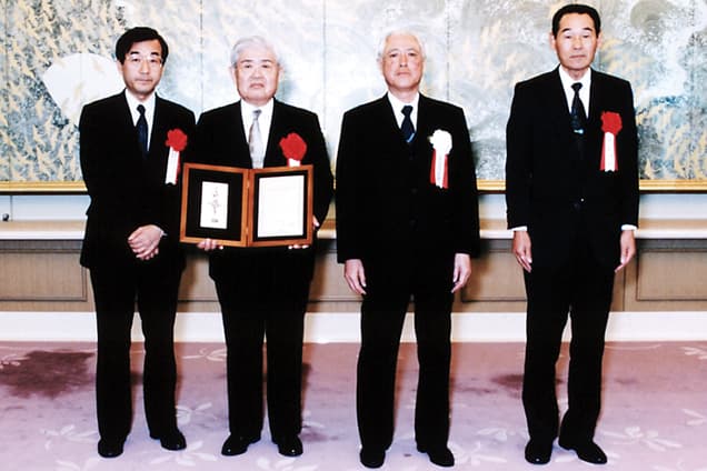
20-inch photomultiplier tubes for neutrino observation were certified as an IEEE Milestone.
Read full story20-inch photomultiplier tubes for neutrino observation were certified as an IEEE Milestone.
The 20-inch diameter photomultiplier tube we developed for Proton decay experiments at Kamiokande was awarded an IEEE Milestone for contributing to neutrinos observation. The IEEE Milestone is an award presented by the IEEE, the world’s largest technical professional organization in the electrical, electronic, information, and communication fields. This award recognizes the historical achievement of technical innovations that must have been developed at least 25 years ago and that have contributed to further development of society and industry. The plaque presented as an IEEE Milestone award was mounted on a rock and installed as a plaque monument at our Toyooka Factory site. The rock used for the plaque monument is Hida gneiss delivered from the Kamioka mine where these cutting-edge experiments in particle physics are still going on. The plaque monument was placed facing toward the Kamioka mine as if it is watching over the next achievement and awaiting new discoveries.
Photo: IEEE Milestone dedication ceremony
Established an affiliated company in Taiwan.
2015
Nobel Prize in physics awarded to Takaaki Kajita, professor of University of Tokyo for research conducted at Super-Kamiokande equipped with a large number of our photomultiplier tubes.
Read full storyNobel Prize in physics awarded to Takaaki Kajita, professor of University of Tokyo for research conducted at Super-Kamiokande equipped with a large number of our photomultiplier tubes.
Photo: 20-inch photomultiplier tube
2017
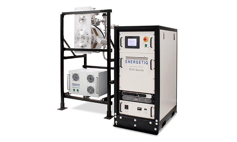
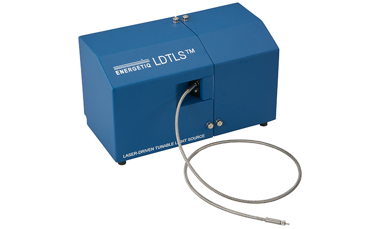
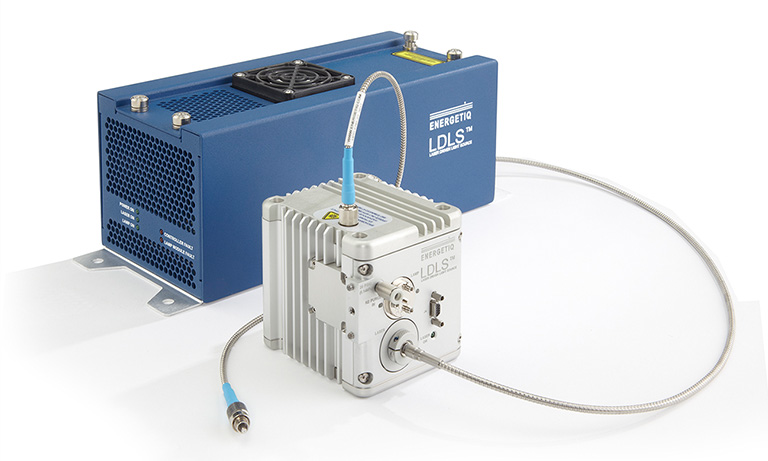
Subsidiary acquisition of Energetiq Technology, Inc. which manufactures and sells light sources for semiconductor testing equipment
2020s
A new challenge to create social and environmental value
2020
Established an affiliated company in Korea.
2022
Tadashi Maruno took office as president and CEO.
- Confirmation
-
It looks like you're in the . If this is not your location, please select the correct region or country below.
You're headed to Hamamatsu Photonics website for JP (English). If you want to view an other country's site, the optimized information will be provided by selecting options below.
In order to use this website comfortably, we use cookies. For cookie details please see our cookie policy.
- Cookie Policy
-
This website or its third-party tools use cookies, which are necessary to its functioning and required to achieve the purposes illustrated in this cookie policy. By closing the cookie warning banner, scrolling the page, clicking a link or continuing to browse otherwise, you agree to the use of cookies.
Hamamatsu uses cookies in order to enhance your experience on our website and ensure that our website functions.
You can visit this page at any time to learn more about cookies, get the most up to date information on how we use cookies and manage your cookie settings. We will not use cookies for any purpose other than the ones stated, but please note that we reserve the right to update our cookies.
1. What are cookies?
For modern websites to work according to visitor’s expectations, they need to collect certain basic information about visitors. To do this, a site will create small text files which are placed on visitor’s devices (computer or mobile) - these files are known as cookies when you access a website. Cookies are used in order to make websites function and work efficiently. Cookies are uniquely assigned to each visitor and can only be read by a web server in the domain that issued the cookie to the visitor. Cookies cannot be used to run programs or deliver viruses to a visitor’s device.
Cookies do various jobs which make the visitor’s experience of the internet much smoother and more interactive. For instance, cookies are used to remember the visitor’s preferences on sites they visit often, to remember language preference and to help navigate between pages more efficiently. Much, though not all, of the data collected is anonymous, though some of it is designed to detect browsing patterns and approximate geographical location to improve the visitor experience.
Certain type of cookies may require the data subject’s consent before storing them on the computer.
2. What are the different types of cookies?
This website uses two types of cookies:
- First party cookies. For our website, the first party cookies are controlled and maintained by Hamamatsu. No other parties have access to these cookies.
- Third party cookies. These cookies are implemented by organizations outside Hamamatsu. We do not have access to the data in these cookies, but we use these cookies to improve the overall website experience.
3. How do we use cookies?
This website uses cookies for following purposes:
- Certain cookies are necessary for our website to function. These are strictly necessary cookies and are required to enable website access, support navigation or provide relevant content. These cookies direct you to the correct region or country, and support security and ecommerce. Strictly necessary cookies also enforce your privacy preferences. Without these strictly necessary cookies, much of our website will not function.
- Analytics cookies are used to track website usage. This data enables us to improve our website usability, performance and website administration. In our analytics cookies, we do not store any personal identifying information.
- Functionality cookies. These are used to recognize you when you return to our website. This enables us to personalize our content for you, greet you by name and remember your preferences (for example, your choice of language or region).
- These cookies record your visit to our website, the pages you have visited and the links you have followed. We will use this information to make our website and the advertising displayed on it more relevant to your interests. We may also share this information with third parties for this purpose.
Cookies help us help you. Through the use of cookies, we learn what is important to our visitors and we develop and enhance website content and functionality to support your experience. Much of our website can be accessed if cookies are disabled, however certain website functions may not work. And, we believe your current and future visits will be enhanced if cookies are enabled.
4. Which cookies do we use?
There are two ways to manage cookie preferences.
- You can set your cookie preferences on your device or in your browser.
- You can set your cookie preferences at the website level.
If you don’t want to receive cookies, you can modify your browser so that it notifies you when cookies are sent to it or you can refuse cookies altogether. You can also delete cookies that have already been set.
If you wish to restrict or block web browser cookies which are set on your device then you can do this through your browser settings; the Help function within your browser should tell you how. Alternatively, you may wish to visit www.aboutcookies.org, which contains comprehensive information on how to do this on a wide variety of desktop browsers.
5. What are Internet tags and how do we use them with cookies?
Occasionally, we may use internet tags (also known as action tags, single-pixel GIFs, clear GIFs, invisible GIFs and 1-by-1 GIFs) at this site and may deploy these tags/cookies through a third-party advertising partner or a web analytical service partner which may be located and store the respective information (including your IP-address) in a foreign country. These tags/cookies are placed on both online advertisements that bring users to this site and on different pages of this site. We use this technology to measure the visitors' responses to our sites and the effectiveness of our advertising campaigns (including how many times a page is opened and which information is consulted) as well as to evaluate your use of this website. The third-party partner or the web analytical service partner may be able to collect data about visitors to our and other sites because of these internet tags/cookies, may compose reports regarding the website’s activity for us and may provide further services which are related to the use of the website and the internet. They may provide such information to other parties if there is a legal requirement that they do so, or if they hire the other parties to process information on their behalf.
If you would like more information about web tags and cookies associated with on-line advertising or to opt-out of third-party collection of this information, please visit the Network Advertising Initiative website http://www.networkadvertising.org.
6. Analytics and Advertisement Cookies
We use third-party cookies (such as Google Analytics) to track visitors on our website, to get reports about how visitors use the website and to inform, optimize and serve ads based on someone's past visits to our website.
You may opt-out of Google Analytics cookies by the websites provided by Google:
https://tools.google.com/dlpage/gaoptout?hl=en
As provided in this Privacy Policy (Article 5), you can learn more about opt-out cookies by the website provided by Network Advertising Initiative:
http://www.networkadvertising.org
We inform you that in such case you will not be able to wholly use all functions of our website.
Close