![]()
Products


We are actively taking measures to improve product quality levels.
Applications


Why Hamamatsu?
Support


Our company


Investors


Japan (EN)
Select your region or country.
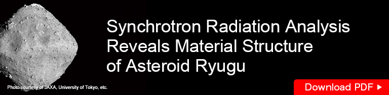
Establishment of absolute photoluminescence (PL) quantum yield measurement method and research on organic optoelectronics
Published June 10, 2025
The Center for Organic Photonics and Electronics Research (OPERA), Kyushu University, is engaged in the research and development of next-generation organic semiconductor devices, including organic light-emitting diode (OLED) devices. In 2012, they succeeded in creating the world's first 3rd-generation organic electroluminescence (EL) emission material called Thermally Activated Delayed Fluorescence (TADF) molecules, leading the field of organic optoelectronics research. Various measurement methods are required to evaluate organic optoelectronic materials and devices, including PL quantum yield measurements and transient luminescence characteristic measurements. For these evaluations, they have used our Quantaurus series and streak cameras.
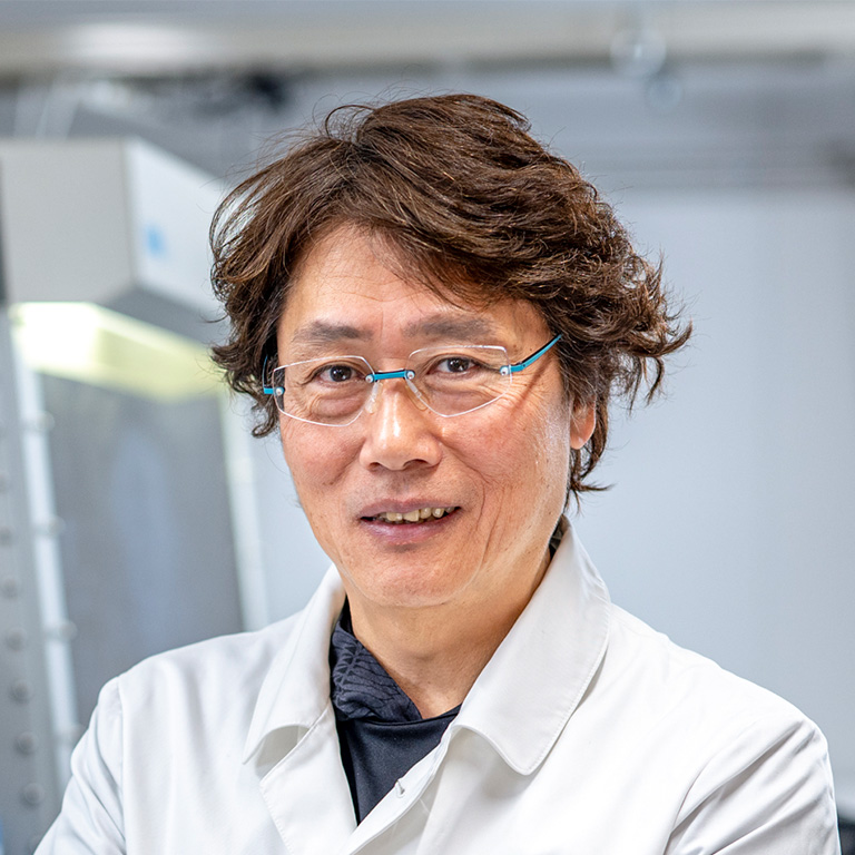
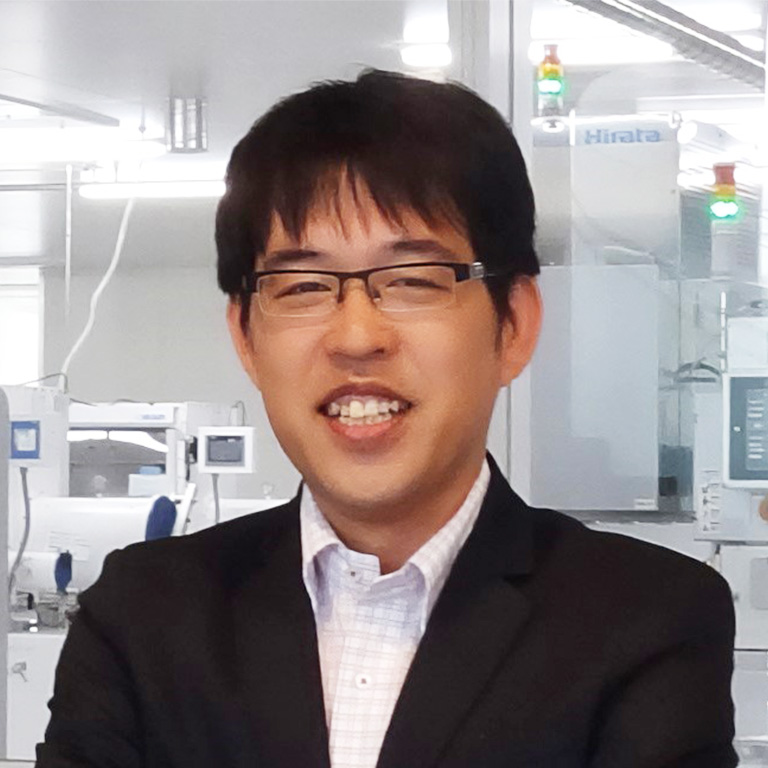
We interviewed Prof. Chihaya Adachi, Director of the Center, and Assoc. Prof. Hajime Nakanotani about establishing absolute photoluminescence quantum yield measurement methods, the impact of our Quantaurus series on their research, and their prospects for future research.
- About research
- Background to the establishment of the PL quantum yield measurement method for solids
- Impact on research after establishment of absolute PL quantum yield measurement method
- Hamamatsu Photonics products in fluorescence lifetime measurement
- Measurement example
- Research prospects
- About Kyulux, Inc.
- About KOALA Tech Inc.
- Researcher profiles
About research
Could you tell us about your research and background?
Prof. Adachi: Our center researches organic optoelectronics, including OLEDs, and develops new semiconductor materials, new device structures based on these materials, and new devices. In 2012, our group succeeded in the world's first creation of TADF molecules, the 3rd generation of organic electroluminescent materials. In 2015, we launched a start-up company (Kyulux) to develop light-emitting devices based on this technology. In 2019, KOALA Tech, Inc. was established to commercialize the organic semiconductor laser diode, which was also successfully developed by the center as a world pioneer. We currently work as a technical advisor to these companies in commercializing and mass-producing materials and devices.
I have been consistently researching OLEDs since around 1987, when I was a graduate student. At that time, there were only a few OLED researchers worldwide. But I believed that challenging a subject that no one else was doing would be of great value. After my graduate studies, I joined a manufacturer and continued my research. A major turning point was research on phosphorescence in the laboratory of Dr. Stephen R. Forrest at Princeton University, to which I later transferred. It was here that the development of OLEDs using second-generation phosphorescent materials began, and by around 2000, I could increase the conversion efficiency to almost 100%.
After that, I returned to Japan and continued researching at Chitose University of Science and Technology. There, I decided to create a new material that would be competitive with phosphorescent materials and succeeded in developing the TADF material. The advantage of this material is that it does not use rare metals, so it can make OLED devices at a lower cost than devices using second-generation phosphorescent materials. Currently, we are working on the practical application of devices based on this TADF material and the research and development of various materials and devices other than OLEDs, such as perovskite solar cells and organic laser diodes.
Professor Chihaya Adachi

Associate Professor Hajime Nakanotani
Background to the establishment of the PL quantum yield measurement method for solids
One method for evaluating luminescent materials, such as OLEDs, is to measure PL quantum yields. However, I understand that this measurement method was not established then. Could you explain how the current PL quantum yield measurement method was established?
Prof. Adachi: At that time, various measurement methods for PL quantum yields of solid materials were reported in the literature. However, the PL quantum yield values varied significantly across different publications, even for the same sample, and there was no established standard method. The only established method was the 'relative method', which involved measuring a standard solution with known PL quantum yield and a sample solution with unknown quantum yield under identical conditions, then comparing these values to determine the relative PL quantum yield of the sample solution. However, this method was limited to measuring solutions and could not be used to evaluate solid materials such as OLEDs.
Under these circumstances, in our laboratory, Dr. Yuichiro Kawamura, a researcher in the JST CREST project, led the development of a measurement system that combined an integrating sphere method reported in the literature with a Hamamatsu Photonics spectrometer (PMA-10). Subsequently, we collaborated with Hamamatsu Photonics to develop an absolute PL quantum yield measurement system. To validate this system, we worked jointly with Hamamatsu Photonics and Tobita Laboratory (currently the Yoshihara Laboratory) at Gunma University to measure the PL quantum yields of fluorescence standard solutions. This helped establish the reliability of the measurements obtained through this method. As a result, we successfully established the 'absolute photoluminescence quantum yield method using an integrating sphere,' enabling solid materials measurement.
Impact on research after establishment of absolute PL quantum yield measurement method
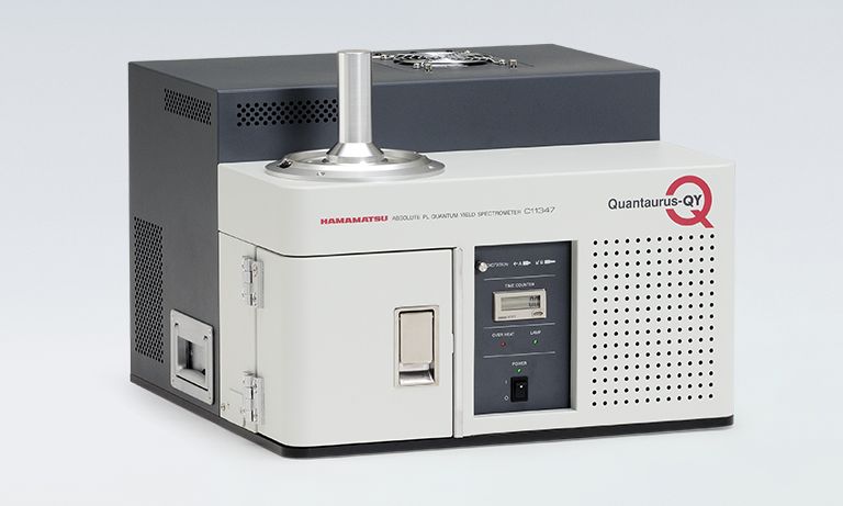
What impact did establishing the absolute photoluminescence quantum yield measurement method have on research? Additionally, how has our Quantaurus-QY® been beneficial to the research?
Prof. Adachi: The most significant impact of establishing the PL quantum yield measurement method is that the luminescence quantum yield values can now be measured correctly. Combining with the value of PL quantum yield and fluorescence lifetime measurements has made it possible to correctly calculate the value of a material's luminescence properties (emission rate constant: kr). As a result, a more detailed characterization of the material is now possible, and the reliability of the characterization has been improved.
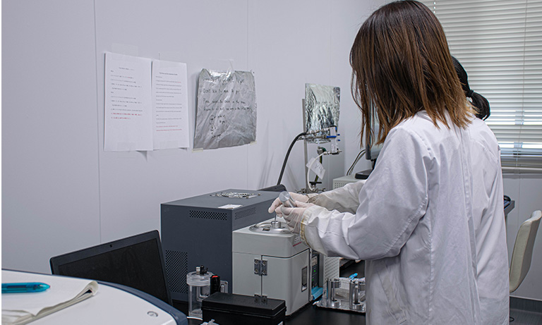
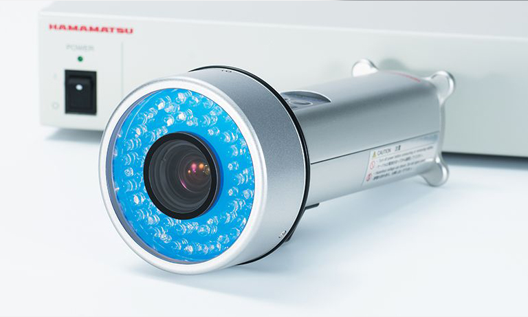
Usage image of Quantaurus-QY
Dr. Nakanotani: From the perspective of promoting research, the three most significant impacts were 1) reduction of measurement time, 2) standardization of work, and 3) reduction of measurement and calculation errors.
Regarding measurement time, the procedure has become simpler compared to the relative method, allowing us to reduce the measurement time.
The procedure has become so simple that anyone can easily perform the measurements by placing the sample in the integrating sphere and taking the measurement, not limited to specialized engineers. Additionally, in the early stages of developing this method, we manually calculated the PL quantum yield values from the spectra obtained by the spectrometer. However, the dedicated software developed by Hamamatsu Photonics to automate PL quantum yield calculation reduced the risk of calculation errors.
Prof. Adachi: The ease of measurement is a very good thing from the perspective of promoting research. However, there are some concerns from the perspective of educating students and researchers. Because anyone can make measurements simply by pushing a button on the device, it is not good for students and researchers to proceed with their research without understanding the mechanisms of measurement, etc. Therefore, we strive to ensure that students and researchers understand these basics before using the device.
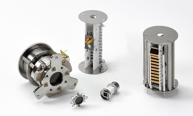
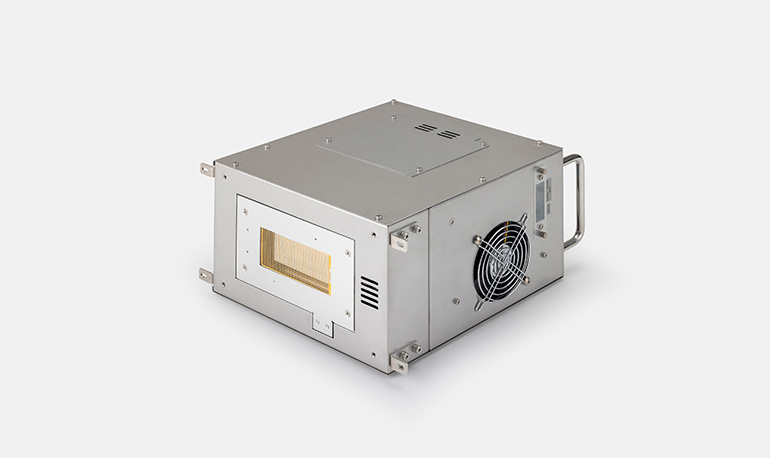
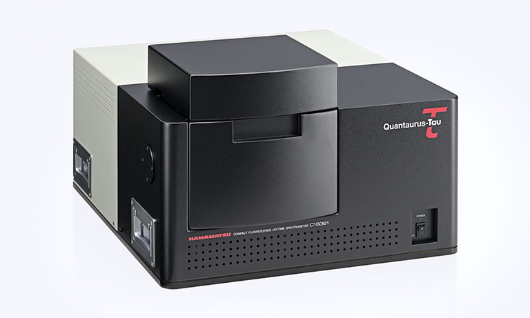
Hamamatsu Photonics products in fluorescence lifetime measurement
The Center for Organic Photonics and Electronics Research (OPERA) also uses the Quantaurus-Tau® compact fluorescence lifetime measurement system and streak cameras to measure materials' fluorescence lifetime and transient absorption.
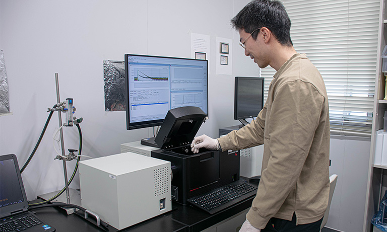
Usage image of Quantaurus-Tau
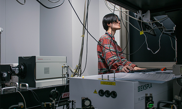
Usage image of Streak camera
Measurement example
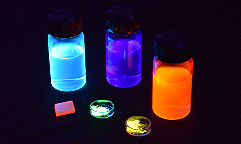
Quantum yield measurement of thermally activated delayed fluorescent materials with high luminous efficiency
Thermally activated delayed fluorescence (TADF) materials are well known as third-generation OLED materials. TADF is the fluorescence generated by the reversed intersystem crossing process (RISC) from the lowest triplet to the singlet states, and the RISC is promoted by the small energy gap between the lowest excited states (ΔEST). A novel TADF material (4CzIPN) was successfully developed by precise molecule design. The material has a small ΔEST, and it shows a high PL quantum yield of 0.94 +/- 0.02.
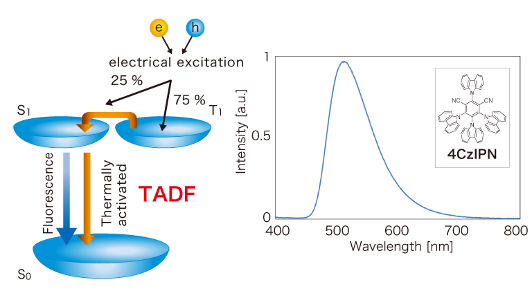
Data courtesy of Prof. Chihaya Adachi, Hajime Nakanotani, Center for Organic Photonics and Electronics Research (OPERA), Kyushu University.
Efficient Near-Infrared Fluorescence in Deuterated Host–Guest System for Near-Infrared Organic Light-Emitting Diodes
PL quantum yield (left) and fluorescence lifetime measurement (right) of near-infrared fluorochromes.
Deuterium substitution increases the PLQY of the NIR fluorophore from 7 % to 15 %.
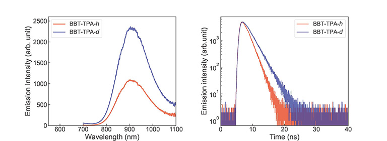
Data courtesy of Prof. Chihaya Adachi, Hajime Nakanotani, Center for Organic Photonics and Electronics Research (OPERA), Kyushu University.
Research prospects
Could you tell us about your research prospects?
Prof. Adachi: We are currently focusing not only on research and development related to OLEDs but also on developing organic solar cells using perovskite and devices using organic charge transfer (CT) complexes. We have been exploring the potential of organic semiconductor devices for many years, and recently, we succeeded in developing a novel organic thermoelectric conversion device that can convert small thermal energy of about tens of meV at room temperature in everyday environments into electricity.
In recent years, the effective use of renewable and unused energy has been sought worldwide. Although thermoelectric conversion devices utilizing waste heat have been partially commercialized, their use remains limited due to various issues. This device, which converts small amounts of thermal energy present at room temperature into electricity, holds the potential to solve energy problems. We consider it a significant achievement of our research that we can now offer this new energy conversion tool to society. Moving forward, we aim to improve the device's performance and stability and pave the way for its practical application.
Dr. Nakanotani: I have recently become interested in materials and devices that emit near-infrared light. Currently, OLEDs are mainly used in the display field, but I would like to create devices that can be used as near-infrared light sources for sensing applications. If we can apply OLEDs to sensors and light sources using near-infrared light, I believe it will lead to business opportunities.

About Kyulux, Inc.
Kyulux, Inc., is a startup company from Kyushu University, established in 2015. It is working on commercializing the OLED technology "Hyperfluorescence™" for use in OLED displays and lighting. Hyperfluorescence™ developed at the Center for Organic Photonics and Electronics Research (OPERA), Kyushu University, is highly anticipated by the display industry as the ultimate OLED technology that achieves high efficiency and high color purity without using rare metals.
Additionally, to accelerate the development of TADF, Kyumatic™, a Materials Informatics (MI) system that combines cutting-edge artificial intelligence (AI) with unique functions introduced by Harvard University in 2016, was applied to materials development to increase development speed dramatically. Kyumatic™ can not only predict material properties but also predict the performance of thin films and devices, and we are focusing on technological development not only for material development and mass production but also for the future development of organic optoelectronic materials.
Prof. Adachi: The Center for Organic Photonics and Electronics Research (OPERA), Kyushu University, is involved in supporting the research and development of Kyulux and is working on high-speed spectroscopic and theoretical analysis of excited states in CT molecular systems, as well as clarification of device degradation mechanisms, to deepen the scientific principles and propose high-performance molecules. We strongly expect that this basic research will improve practical device performance.
About KOALA Tech Inc.
KOALA Tech, Inc., is a start-up company from Kyushu University, established in 2019. This company was established to commercialize the world's first Organic Semiconductor Laser Diode (OSLD) laser technology realized by the Kyushu University Research Center for Advanced Organic Photonics and Electronics (OPERA). OSLDs combine the “flexibility, low environmental impact, low cost, and high wavelength selectivity” of organic electronics with the “high color purity and high light linearity” of lasers.
We have been working on the practical application of OSLDs as a laser light source that is highly compatible with organic electronic device platforms, including OLEDs, which have attracted attention in recent years as high-definition and flexible displays to provide new solutions to customers in the organic semiconductor device field and to contribute to a smart society where people and technology coexist through organic x laser hybrid technology.
Prof. Adachi: The Center for Organic Photonics and Electronics Research (OPERA), Kyushu University, provides cutting-edge academic knowledge and world-class research and development infrastructure through its collaborative research with KOALA Tech. We expect that further advancements and commercialization of organic semiconductor laser research and development will significantly expand the frontier of organic electronics in both academic and industrial fields.
Researcher profiles
Chihaya Adachi
Department of Applied Chemistry, Kyushu University: Professor
Center for Organic Photonics and Electronics Research (OPERA): Director
Mar. 1991
Ph.D., Department of Materials Development Engineering, Graduate School of Engineering Sciences, Kyushu University
Apr. 1991
Researcher, Ricoh Co., Ltd. Chemical Products Technology Research Institute
Aug. 1996
Assistant, Department of Functional Polymer Science, Faculty of Textile Science and Technology, Shinshu University
May. 1999
Researcher, Center for Photonics and Optoelectronic Materials (POEM), Princeton University
Mar. 2001
Assistant Professor, Department of Materials and Photonic Science, School of Photonics Science, Chitose Institute of Science and Technology
Apr. 2004
Professor, Department of Materials and Photonic Science, School of Photonics Science, Chitose Institute of Science and Technology
Oct. 2005
Professor, Center for Future Chemistry, Kyushu University
Apr. 2010
Current post
Hajime Nakanotani
Department of Applied Chemistry, Kyushu University: Associate Professor
Center for Organic Photonics and Electronics Research (OPERA): Vice Director
Mar. 2010
Department of Materials Creation Engineering, Graduate School of Engineering, Kyushu University, Ph.D.
Apr. 2010
Researcher, Ricoh Co., Ltd. Research and Development Headquarters
Apr. 2012
Researcher, Organic Photonics Device Laboratory, Kyushu Institute of Advanced Science and Technology, Public Interest Incorporated Foundation
Visiting Assistant Professor, Center for Futere Chemistry
Apr. 2014
Assistant Professor, Center for Organic Photonics and Electronics Research (OPERA)
Jan. 2015
Department of Applied Chemistry, Kyushu University: Associate Professor
Apr. 2019
Center for Organic Photonics and Electronics Research (OPERA): Vice Director
*The content presented on this page is based on an interview conducted in November 2024.
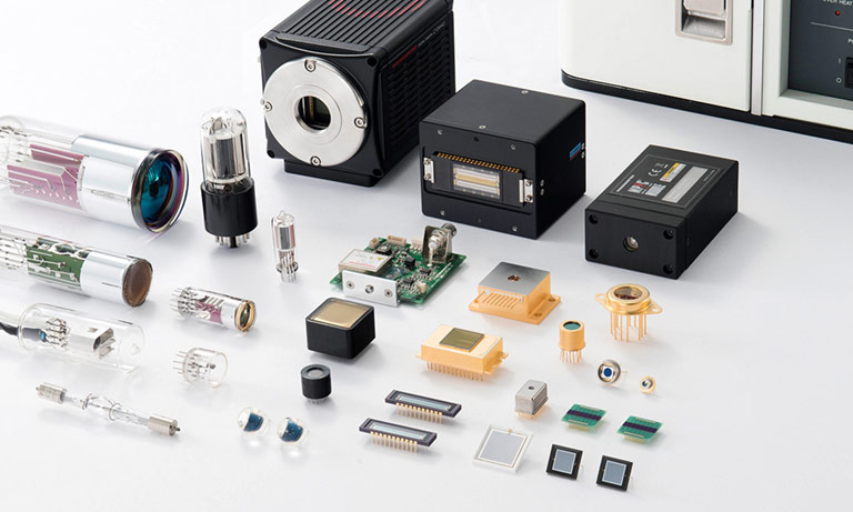
Related product
Compact one-box absolute quantum yield spectrometer for luminescence materials using photoluminescence method. Not only thin materials but also liquid solution and powder can be analyzed. It quickly measures the absolute PL quantum yield, excitation wavelength dependence and PL in a short time.
Compact one-box fluorescence lifetime measurement system to measure fluorescence lifetime and PL spectrum with easy operation and high precision.
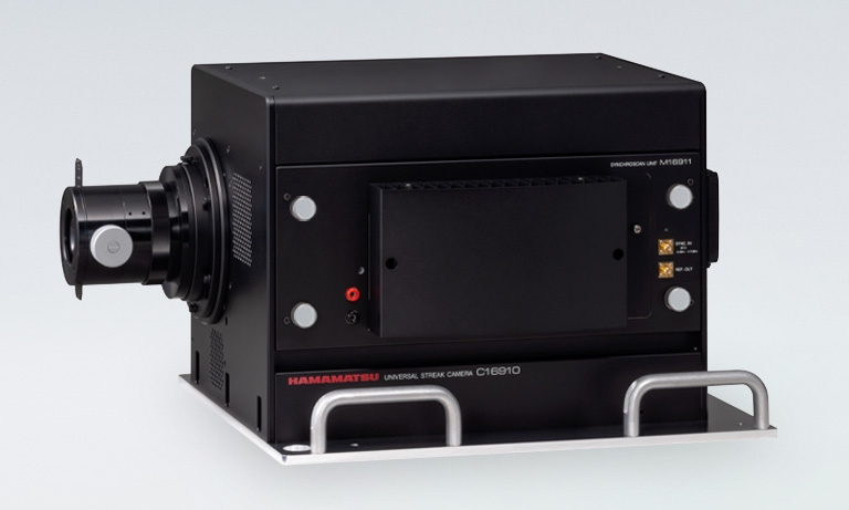
Universal streak camera to cover the picosecond to nanosecond time range with single-shot or synchroscan. It can be configured for various measurement targets.
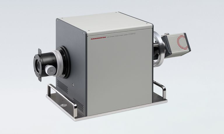
The C13410 is a high dynamic range streak camera that can handle a large number of photo-electrons. This feature enables single-shot measurements of ultra fast phenomena with a dynamic range as high as 10 000 : 1.
- Confirmation
-
It looks like you're in the . If this is not your location, please select the correct region or country below.
You're headed to Hamamatsu Photonics website for JP (English). If you want to view an other country's site, the optimized information will be provided by selecting options below.
In order to use this website comfortably, we use cookies. For cookie details please see our cookie policy.
- Cookie Policy
-
This website or its third-party tools use cookies, which are necessary to its functioning and required to achieve the purposes illustrated in this cookie policy. By closing the cookie warning banner, scrolling the page, clicking a link or continuing to browse otherwise, you agree to the use of cookies.
Hamamatsu uses cookies in order to enhance your experience on our website and ensure that our website functions.
You can visit this page at any time to learn more about cookies, get the most up to date information on how we use cookies and manage your cookie settings. We will not use cookies for any purpose other than the ones stated, but please note that we reserve the right to update our cookies.
1. What are cookies?
For modern websites to work according to visitor’s expectations, they need to collect certain basic information about visitors. To do this, a site will create small text files which are placed on visitor’s devices (computer or mobile) - these files are known as cookies when you access a website. Cookies are used in order to make websites function and work efficiently. Cookies are uniquely assigned to each visitor and can only be read by a web server in the domain that issued the cookie to the visitor. Cookies cannot be used to run programs or deliver viruses to a visitor’s device.
Cookies do various jobs which make the visitor’s experience of the internet much smoother and more interactive. For instance, cookies are used to remember the visitor’s preferences on sites they visit often, to remember language preference and to help navigate between pages more efficiently. Much, though not all, of the data collected is anonymous, though some of it is designed to detect browsing patterns and approximate geographical location to improve the visitor experience.
Certain type of cookies may require the data subject’s consent before storing them on the computer.
2. What are the different types of cookies?
This website uses two types of cookies:
- First party cookies. For our website, the first party cookies are controlled and maintained by Hamamatsu. No other parties have access to these cookies.
- Third party cookies. These cookies are implemented by organizations outside Hamamatsu. We do not have access to the data in these cookies, but we use these cookies to improve the overall website experience.
3. How do we use cookies?
This website uses cookies for following purposes:
- Certain cookies are necessary for our website to function. These are strictly necessary cookies and are required to enable website access, support navigation or provide relevant content. These cookies direct you to the correct region or country, and support security and ecommerce. Strictly necessary cookies also enforce your privacy preferences. Without these strictly necessary cookies, much of our website will not function.
- Analytics cookies are used to track website usage. This data enables us to improve our website usability, performance and website administration. In our analytics cookies, we do not store any personal identifying information.
- Functionality cookies. These are used to recognize you when you return to our website. This enables us to personalize our content for you, greet you by name and remember your preferences (for example, your choice of language or region).
- These cookies record your visit to our website, the pages you have visited and the links you have followed. We will use this information to make our website and the advertising displayed on it more relevant to your interests. We may also share this information with third parties for this purpose.
Cookies help us help you. Through the use of cookies, we learn what is important to our visitors and we develop and enhance website content and functionality to support your experience. Much of our website can be accessed if cookies are disabled, however certain website functions may not work. And, we believe your current and future visits will be enhanced if cookies are enabled.
4. Which cookies do we use?
There are two ways to manage cookie preferences.
- You can set your cookie preferences on your device or in your browser.
- You can set your cookie preferences at the website level.
If you don’t want to receive cookies, you can modify your browser so that it notifies you when cookies are sent to it or you can refuse cookies altogether. You can also delete cookies that have already been set.
If you wish to restrict or block web browser cookies which are set on your device then you can do this through your browser settings; the Help function within your browser should tell you how. Alternatively, you may wish to visit www.aboutcookies.org, which contains comprehensive information on how to do this on a wide variety of desktop browsers.
5. What are Internet tags and how do we use them with cookies?
Occasionally, we may use internet tags (also known as action tags, single-pixel GIFs, clear GIFs, invisible GIFs and 1-by-1 GIFs) at this site and may deploy these tags/cookies through a third-party advertising partner or a web analytical service partner which may be located and store the respective information (including your IP-address) in a foreign country. These tags/cookies are placed on both online advertisements that bring users to this site and on different pages of this site. We use this technology to measure the visitors' responses to our sites and the effectiveness of our advertising campaigns (including how many times a page is opened and which information is consulted) as well as to evaluate your use of this website. The third-party partner or the web analytical service partner may be able to collect data about visitors to our and other sites because of these internet tags/cookies, may compose reports regarding the website’s activity for us and may provide further services which are related to the use of the website and the internet. They may provide such information to other parties if there is a legal requirement that they do so, or if they hire the other parties to process information on their behalf.
If you would like more information about web tags and cookies associated with on-line advertising or to opt-out of third-party collection of this information, please visit the Network Advertising Initiative website http://www.networkadvertising.org.
6. Analytics and Advertisement Cookies
We use third-party cookies (such as Google Analytics) to track visitors on our website, to get reports about how visitors use the website and to inform, optimize and serve ads based on someone's past visits to our website.
You may opt-out of Google Analytics cookies by the websites provided by Google:
https://tools.google.com/dlpage/gaoptout?hl=en
As provided in this Privacy Policy (Article 5), you can learn more about opt-out cookies by the website provided by Network Advertising Initiative:
http://www.networkadvertising.org
We inform you that in such case you will not be able to wholly use all functions of our website.
Close