![]()
Products


We are actively taking measures to improve product quality levels.
Applications


Why Hamamatsu?
Support


Our company


Investors


Japan (EN)
Select your region or country.
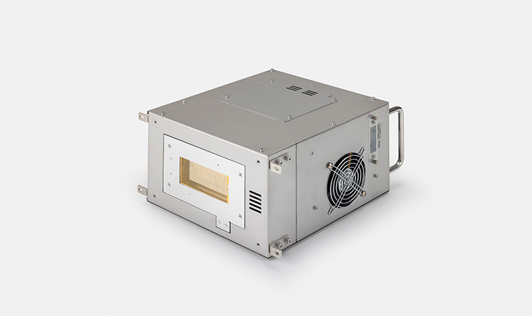
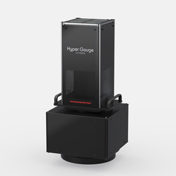
HyperGauge Thickness measurement system
C17319-11
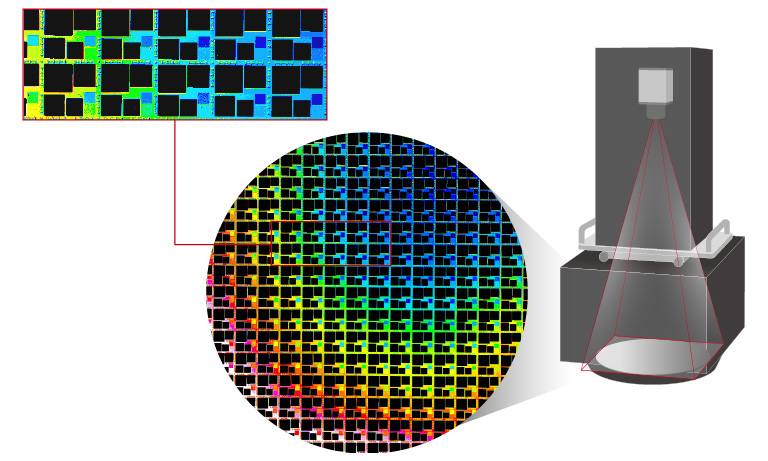
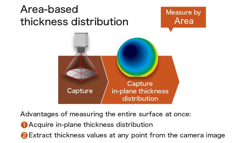
Measure thickness distribution of a 300 mm wafer in only 5 seconds
The HyperGauge® Thickness measurement system C17319-11 employs a spectroscopic interference method for precise film thickness measurement. Equipped with the λ-Capture® technology, which detects wavelength shifts using high-sensitivity cameras without a spectrometer, it can measure the entire film thickness of up to 300 mm wafers in as little as 5 seconds.
HyperGauge is registered trademark of Hamamatsu Photonics K.K. (EU, Japan, UK, USA).
λ-Capture is registered trademark of Hamamatsu Photonics K.K. (EU, Korea, Japan, Taiwan, UK, USA).
Snapshot of in-plane thickness distribution
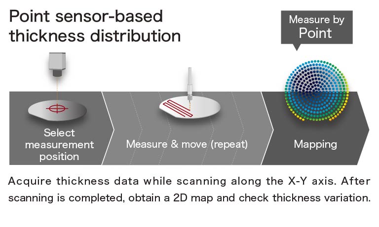
Compared to point sensor systems, HyperGauge Thickness measurement system C17319-11 delivers dramatically faster acquisition of thickness distribution. Combining high spatial resolution with excellent measurement repeatability, the system achieves the accuracy required for inspecting not only bare wafers but also patterned wafers.
Acquire thickness distribution in only 5 seconds
By adopting Hamamatsu’s proprietary wavelength detection technology, λ-Capture, combined with high-sensitivity cameras, the system enables area-based thickness measurement. It captures the in-plane thickness distribution of wafers up to 300 mm in diameter in as little as 5 seconds. Since the entire wafer surface is imaged at once, it simplifies measurement point selection and alignment compared to point sensor systems.
Boost productivity with fast uniformity measurement
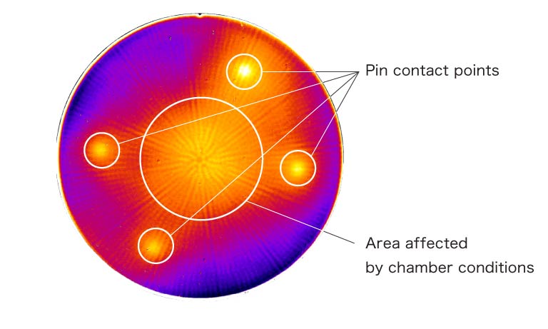
In semiconductor manufacturing processes, variations in film thickness can occur on wafers due to factors such as pin temperature inside the chamber. These thickness non-uniformities negatively affect product quality, making it essential to equalize film thickness between process steps. With point sensor systems, the number of measurement points is limited by time constraints, making it difficult to fully capture in-plane thickness distribution. By adopting an area-based approach, our system measures in-plane thickness distribution from approximately 750 000 points in only 5 seconds. This enables shorter process times for improved productivity and better yield through comprehensive thickness distribution analysis. Fast in-plane uniformity measurement significantly contributes to both productivity and quality in semiconductor manufacturing.
Chamber-induced thickness variation
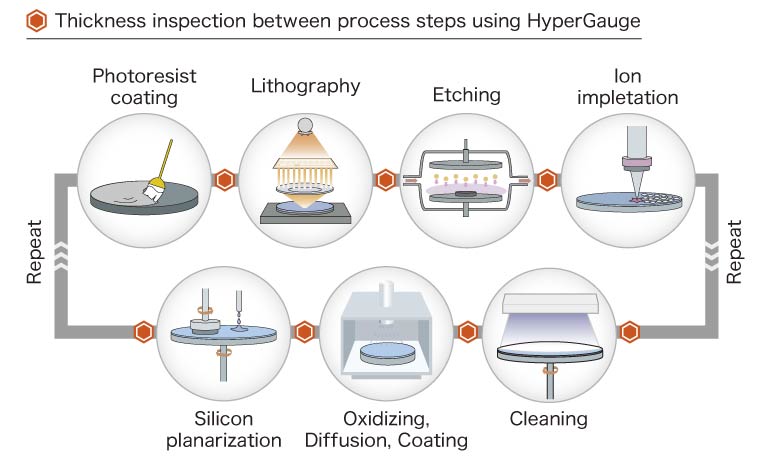
Thickness inspection in semiconductor process
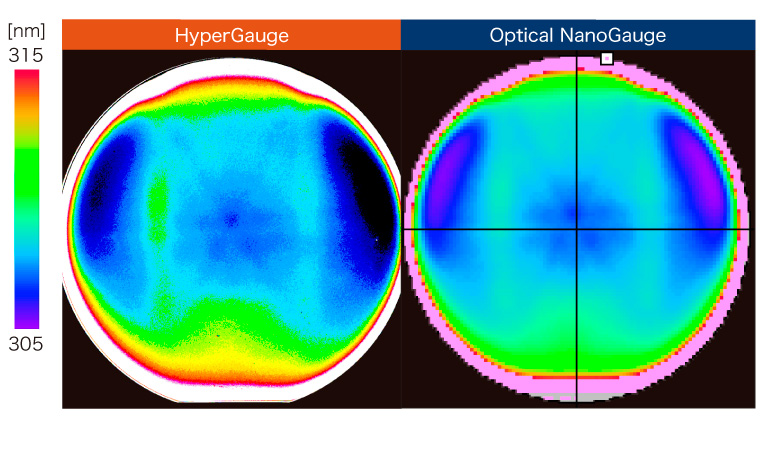
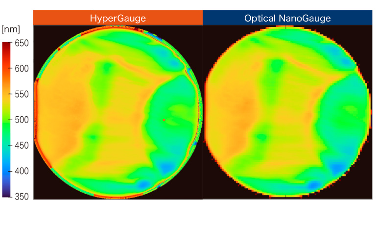
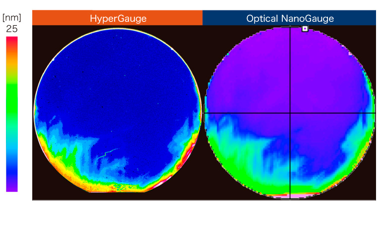
Measurement example
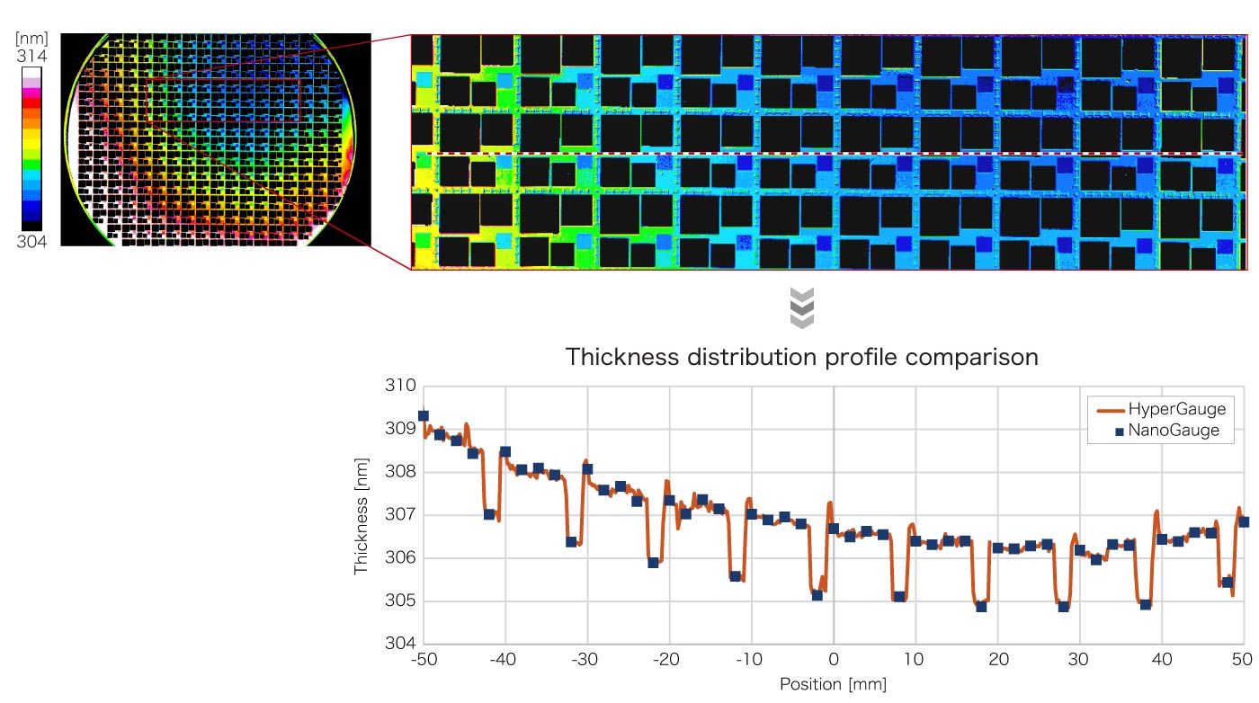
Pattern evaluation (comparison of thickness distribution profiles)
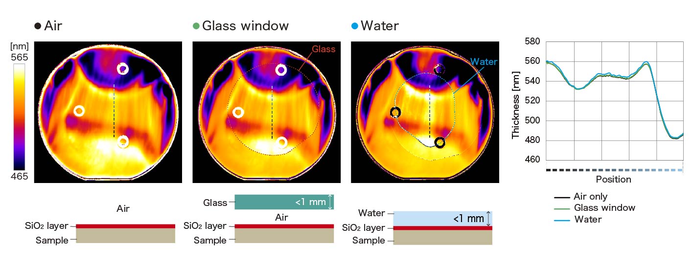
We acquired the thickness distribution between patterns and compared the thickness distribution profiles of Optical NanoGauge, which uses a point sensor method, and HyperGauge, which uses an area-based method. The results show that HyperGauge can measure film thickness with accuracy comparable to the point sensor method.
Large non-uniformity: SiO2 300 nm
Small non-uniformity: SiO2 500 nm
Ultra-thin film: SiO2 10 nm
Pattern evaluation: SiOx2 300 nm

Through water & glass: SiO2 500 nm
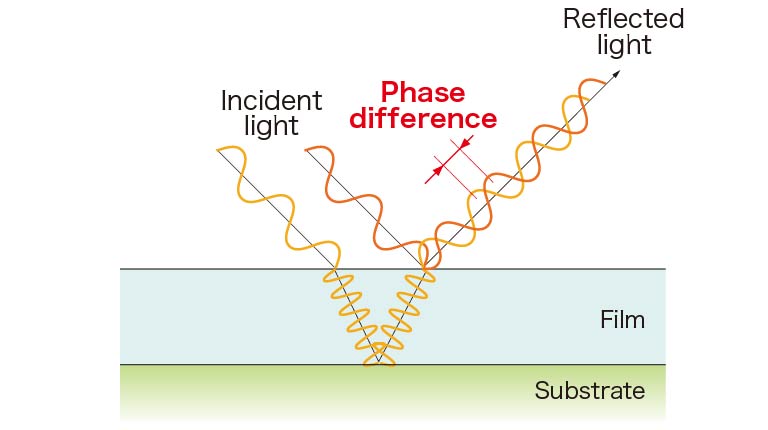
Measurement principle
HyperGauge employs spectroscopic interferometry. This method analyzes the reflections from thin-film samples to measure film thickness. The interference spectrum shifts depending on the film thickness.
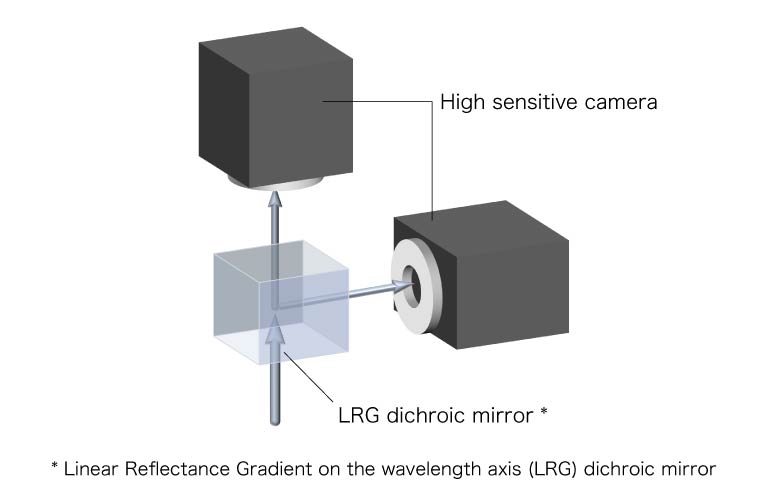
λ-Capture technology for high speed wavelength measurement
λ-Capture is a proprietary wavelength detection technology that enables wavelength measurement without using a spectrometer. When performing wavelength measurement of the entire wafer, point measurement with a conventional spectrometer or line measurement with an imaging spectrometer takes an enormous amount of time.
By utilizing two high-sensitivity cameras, it measures wavelengths across an area, allowing high-speed spectroscopic measurement of the entire wafer surface. By incorporating this technology into HyperGauge, in-plane film thickness distribution measurement across the wafer is achieved in just 5 seconds.
Specifications
| Product number | C17319-11 |
|---|---|
| Measurement film thickness range | 10 nm to 1000 nm |
| Measurement accuracy | Film thickness 10 nm to 100 nm: ±1 nm Film thickness 100 nm to 1000 nm: ±1 % |
| Measurement reproducibility | Film thickness 10 nm to 100 nm (96 integrations): 0.1 nm Film thickness 100 nm to 1000 nm (96 integrations): ±0.1 % |
| Stability | Temperature dependence: Environmental temperature variation +20℃ to + 30℃: ±1 % Height dependency (5 mm height variation): ±1 % Long-term stability (1 hour after startup): ±0.5 % |
| Field of view | Full 300 mm wafer surface |
| Spatial resolution | 0.3 mm/pixel |
| Working distance | Field lens botton-to-sample surface distance: 30 nm to 100 mm |
| Analysis | λ-Capture analysis |
| Measurement time (including analysis time)*1 | 5 seconds |
| External communication interface | Camera Link, RS-232C |
| Power supply voltage | DC 24 V |
| Power consumption | Approx. 40 W |
*1 Depends on measurement and analysis conditions.
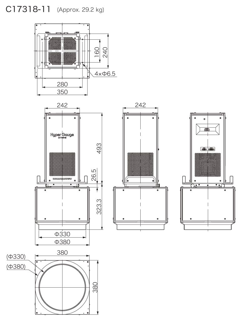
Dimensions
- Confirmation
-
It looks like you're in the . If this is not your location, please select the correct region or country below.
You're headed to Hamamatsu Photonics website for JP (English). If you want to view an other country's site, the optimized information will be provided by selecting options below.
In order to use this website comfortably, we use cookies. For cookie details please see our cookie policy.
- Cookie Policy
-
This website or its third-party tools use cookies, which are necessary to its functioning and required to achieve the purposes illustrated in this cookie policy. By closing the cookie warning banner, scrolling the page, clicking a link or continuing to browse otherwise, you agree to the use of cookies.
Hamamatsu uses cookies in order to enhance your experience on our website and ensure that our website functions.
You can visit this page at any time to learn more about cookies, get the most up to date information on how we use cookies and manage your cookie settings. We will not use cookies for any purpose other than the ones stated, but please note that we reserve the right to update our cookies.
1. What are cookies?
For modern websites to work according to visitor’s expectations, they need to collect certain basic information about visitors. To do this, a site will create small text files which are placed on visitor’s devices (computer or mobile) - these files are known as cookies when you access a website. Cookies are used in order to make websites function and work efficiently. Cookies are uniquely assigned to each visitor and can only be read by a web server in the domain that issued the cookie to the visitor. Cookies cannot be used to run programs or deliver viruses to a visitor’s device.
Cookies do various jobs which make the visitor’s experience of the internet much smoother and more interactive. For instance, cookies are used to remember the visitor’s preferences on sites they visit often, to remember language preference and to help navigate between pages more efficiently. Much, though not all, of the data collected is anonymous, though some of it is designed to detect browsing patterns and approximate geographical location to improve the visitor experience.
Certain type of cookies may require the data subject’s consent before storing them on the computer.
2. What are the different types of cookies?
This website uses two types of cookies:
- First party cookies. For our website, the first party cookies are controlled and maintained by Hamamatsu. No other parties have access to these cookies.
- Third party cookies. These cookies are implemented by organizations outside Hamamatsu. We do not have access to the data in these cookies, but we use these cookies to improve the overall website experience.
3. How do we use cookies?
This website uses cookies for following purposes:
- Certain cookies are necessary for our website to function. These are strictly necessary cookies and are required to enable website access, support navigation or provide relevant content. These cookies direct you to the correct region or country, and support security and ecommerce. Strictly necessary cookies also enforce your privacy preferences. Without these strictly necessary cookies, much of our website will not function.
- Analytics cookies are used to track website usage. This data enables us to improve our website usability, performance and website administration. In our analytics cookies, we do not store any personal identifying information.
- Functionality cookies. These are used to recognize you when you return to our website. This enables us to personalize our content for you, greet you by name and remember your preferences (for example, your choice of language or region).
- These cookies record your visit to our website, the pages you have visited and the links you have followed. We will use this information to make our website and the advertising displayed on it more relevant to your interests. We may also share this information with third parties for this purpose.
Cookies help us help you. Through the use of cookies, we learn what is important to our visitors and we develop and enhance website content and functionality to support your experience. Much of our website can be accessed if cookies are disabled, however certain website functions may not work. And, we believe your current and future visits will be enhanced if cookies are enabled.
4. Which cookies do we use?
There are two ways to manage cookie preferences.
- You can set your cookie preferences on your device or in your browser.
- You can set your cookie preferences at the website level.
If you don’t want to receive cookies, you can modify your browser so that it notifies you when cookies are sent to it or you can refuse cookies altogether. You can also delete cookies that have already been set.
If you wish to restrict or block web browser cookies which are set on your device then you can do this through your browser settings; the Help function within your browser should tell you how. Alternatively, you may wish to visit www.aboutcookies.org, which contains comprehensive information on how to do this on a wide variety of desktop browsers.
5. What are Internet tags and how do we use them with cookies?
Occasionally, we may use internet tags (also known as action tags, single-pixel GIFs, clear GIFs, invisible GIFs and 1-by-1 GIFs) at this site and may deploy these tags/cookies through a third-party advertising partner or a web analytical service partner which may be located and store the respective information (including your IP-address) in a foreign country. These tags/cookies are placed on both online advertisements that bring users to this site and on different pages of this site. We use this technology to measure the visitors' responses to our sites and the effectiveness of our advertising campaigns (including how many times a page is opened and which information is consulted) as well as to evaluate your use of this website. The third-party partner or the web analytical service partner may be able to collect data about visitors to our and other sites because of these internet tags/cookies, may compose reports regarding the website’s activity for us and may provide further services which are related to the use of the website and the internet. They may provide such information to other parties if there is a legal requirement that they do so, or if they hire the other parties to process information on their behalf.
If you would like more information about web tags and cookies associated with on-line advertising or to opt-out of third-party collection of this information, please visit the Network Advertising Initiative website http://www.networkadvertising.org.
6. Analytics and Advertisement Cookies
We use third-party cookies (such as Google Analytics) to track visitors on our website, to get reports about how visitors use the website and to inform, optimize and serve ads based on someone's past visits to our website.
You may opt-out of Google Analytics cookies by the websites provided by Google:
https://tools.google.com/dlpage/gaoptout?hl=en
As provided in this Privacy Policy (Article 5), you can learn more about opt-out cookies by the website provided by Network Advertising Initiative:
http://www.networkadvertising.org
We inform you that in such case you will not be able to wholly use all functions of our website.
Close