Japan (EN)
Select your region or country.
P
- p.e. (photon equivalent)
- Passive alignment
- Phosphor screen
- Photocathode material
- Photoconductive detector
- Photoelectric effect
- Photon counting
- Photon detection efficiency (PDE)
- Photoresponse nonuniformity
- Photosensitive area
- Photosensitivity
- Photovoltaic detector
- Position detection error
- Position resolution (ΔR)
- Power dissipation
- Propagation delay time
- PSD (position sensitive detector)
- Pseudo-random pattern
p.e. (photon equivalent)
This represents the detection level per photon. A 1 p.e. pulse, for example, is equivalent to the pulse obtained when one photon is detected.
Passive alignment
Precise mechanical positioning for coupling alignment between two or more optical elements during optical module assembly. Since the positioning of optical elements usually requires accuracy ranging from submicrons to several microns, highly precise metalization patterns and V-grooves formed by semiconductor process technology are utilized as the positioning reference. In contrast to passive alignment, active alignment performs the positioning of optical modules or fibers while making the optical modules emit light by simulating actual operation (for instance, operating a laser diode to emit light) and monitoring the emitted light in order to obtain the required characteristics of the optical modules.
Phosphor screen
A scintillator in the form of a thin sheet. This is usually fabricated by depositing scintillator material on a support substrate and covering it with protective film.
Photocathode material
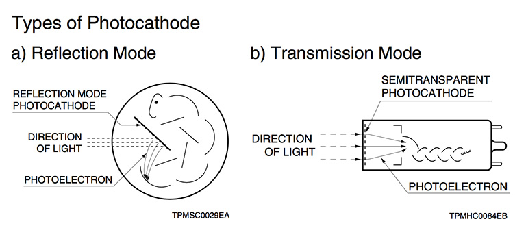
The photocathode is a photoemissive surface usually consisting of alkali metals with very low work functions. The photocathode materials most commonly used in photomultiplier tubes are as follows:
1.Ag-O-Cs. The transmission-mode photocathode using this material is designated S-1 and sensitive from the range of visible light to infrared radiation (300 nm to 1000 nm). The reflection mode covers a slightly narrower range from 300 nm to 1100 nm. Since Ag-O-Cs has comparatively high thermionic dark emission, photomultiplier tubes of this photocathode material are chiefly used for detection in the infrared region with the photocathode cooled.
2.GaAs GaAs activated in cesium is also used as a photocathode. The spectral response of this photocathode material usually covers a wider spectral response range than multialkali, from ultraviolet to 930 nm, which is comparatively flat over the range between 300 nm and 850 nm.
3.InGaAs.This photocathode material has greater extended sensitivity in the infrared range than GaAs. Moreover, in the range between 900 nm and 1000 nm, InGaAs has a much higher S/N ratio than Ag-O-Cs. Some photocathodes can operate at 1700 nm.
4.Sb-Cs. Sb-Cs has a spectral response in the ultraviolet to visible range and is mainly used in reflection-mode photocathodes.
5. Bialkali (Sb-Rb-Cs, Sb-K-Cs). These materials have a spectral response range similar to the Sb-Cs photocathode, but have higher sensitivity and lower dark current than Sb-Cs. They also have a blue sensitivity index matching the scintillation flashes of NaI scintillators and so are frequently used for radiation measurement using scintillation counting.
6. High temperature bialkali or low noise bialkali (Na-K-Sb). This is particularly useful at higher operating temperatures since it can withstand up to 175 °C. At room temperatures, this photocathode operates with very low dark current, making it ideal for use in photon counting applications.
7. Multialkali (Na-K-Sb-Cs). The multialkali photocathode has a high, wide spectral response from the ultraviolet to near infrared region. It is widely used for broad-band spectrophotometers and photon counting applications. The long wavelength response can be extended to 930 nm by a special photocathode activation processing.
8.Cs-Te, Cs-I. These materials are sensitive to vacuum UV and UV rays but not to visible light and are therefore referred to as solar blind. Cs-Te is quite insensitive to wavelengths longer than 320 nm, and Cs-I to those longer than 200 nm.
Photoconductive detector
A photosensor which increases its electric conductivity when illuminated with light. An external power supply is needed to operate a photoconductive detector. Photoconductive detectors include MCT (HgCdTe), PbS, PbSe, etc.
Photoelectric effect
A phenomenon in which a substance absorbs light and generates free electrons.
Photon counting
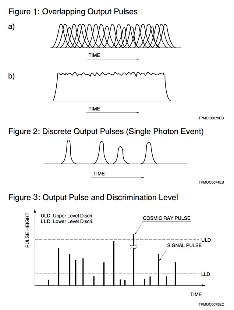
PMTs have extremely high gain low noise amplifiers. The mechanism is capable of amplifying a single electron into a detectable signal. Usually these single electron pulses are summed and read as a DC current. However it is possible to count the single electron pulses; since each pulse represents a photon this method is known as photon counting. It offers some advantages in noise and stability and the convenience of digital detection.
Photon detection efficiency (PDE)
This is a measure of what percent of the incident photons were detected. PDE is expressed by the following equation. The avalanche probability (Pa) becomes larger as the reverse voltage is increased. $$PDE = QE \cdot fg \cdot Pa$$
- QE: quantum efficiency
- fg: geometric factor
- Pa: avalanche probability
Photoresponse nonuniformity
Each of the photodiodes arrayed in an image sensor or CCD is carefully fabricated to provide uniform performance, but each also exhibits some small nonuniformity in terms of sensitivity. This may be due to crystal flaws in the silicon substrate, variations in the wafer process and diffusion in the manufacturing process. This nonuniformity is often called the photoresponse nonuniformity.
Photosensitive area
The area in a device that actually collects light and converts it to electrons. In our data photosensitive areas which are circular are noted with one dimension and quadrilateral squares with two dimensions. Some PMT dimensions are described as 2π, square or hexagonal.
Photosensitivity
The ratio of photocurrent expressed in amperes (A) or output voltage expressed in volts (V) to the incident light level expressed in watts (W). Photosensitivity is represented as an absolute sensitivity (A/W or V/W) or as a relative sensitivity (%) to the peak wavelength sensitivity normalized to 100. We usually define the spectral response range as the range in which the relative sensitivity is higher than 5% or 10% of the peak sensitivity.
Photovoltaic detector
A semiconductor photosensor generating an electrical current or voltage when light is illuminated on its PN junction. It is capable of operating without power supplied from an external source. Photovoltaic detectors include Si, InGaAs, GaAsP, GaAs, InAs, InSb, etc.
Position detection error
When a light spot irradiates onto a PSD and the resulting current extracted from each output terminal of the PSD is equal, the incident position of the light spot is called the electrical center of the PSD. By considering this electrical center as the origin, the position detection error is defined as the difference between the position at which the light spot is actually incident on the PSD and the position calculated from the photocurrents. We measure the position detection error under the following conditions:
- Light source: λ=890 nm
- Light spot size: Φ200 µm
- Photocurrent: 10 µA
Position resolution (ΔR)
The minimum detectable displacement of a light spot incident on the photosensitive surface of a PSD, expressed as a distance on the photosensitive surface of the PSD. This position resolution is determined by the S/N, which is calculated by: PSD resistance length x noise/signal. We define the position resolution calculated based on root-mean-square (rms) noise measured under the following conditions:
- Interelectrode resistance: See characteristic table in our datasheets.
- Photocurrent: 1 µA
- Frequency bandwidth: 1 kHz
- Equivalent input voltage noise of circuit: 1 µV
Power dissipation
The maximum power consumption allowed for a device, calculated from the upper temperature limit of the package and chip. In most cases, this is determined by heat-vulnerable components included in the device. Using a coefficient called “derating” makes it possible to calculate the absolute maximum rating for the power dissipation at the temperature at which the device will actually be used. For example, if a power dissipation of 500 mW is defined as the absolute maximum rating at 25 °C and the derating is 5 mW/°C, then the absolute maximum rating at 85 °C will be: 500 mW - 5 mW/°C x (85 °C - 25 °C) = 200 mW.
Propagation delay time
The time required for a signal to travel from the transmitted point to the received point. This term generally indicates the total delay time in the circuit and optical elements, and the delay time in a medium (optical fiber, etc.). The propagation delay time that changes is termed the jitter or wander. Jitter is the fluctuation in propagation delay time that occurs in a short period of time and mainly results from noise. Wander is a long-term fluctuation chiefly caused by thermal factors.
PSD (position sensitive detector)
A position sensitive detector (PSD) consists of a monolithic PIN photodiode with a uniform resistance in one or two dimensions. PSDs have many advantages, compared to discrete element detectors, including high position resolution, fast response speed and simple operating circuits. Position data is independent of the size of light spot on the detector. They can be used for non-contact distance measurement, laser beam alignment and optical tracking of an object. PSDs for tracking electrons or high energy particles are also available.
Hamamatsu makes the following:
1D PSD: Monolithic Si detector using surface resistance to provide continuous position information in one dimension.
2D PSD: Monolithic Si detector using surface resistance to provide continuous position information in two dimensions. Certain photomultipliers can also be used to provide two-dimensional position information.
Special types: A number of products can serve the same function as a PSD, but do not fit into the same general category. These include discrete PSD arrays, devices that can switch from being a photodiode to a PSD, non-linear output PSDs and PSD angle sensors. Signal processing circuits. Various types of signal processing circuits are available for the tracking of a light spot independent of incident light level. Boards are available for one or two-dimensional and either pin-cushion, tetra-lateral or duo-lateral PSDs. The signal processing boards are a compact size and easy to use, no complicated adjustments required. Measurements can be made by simply connecting the PSD and a +15V power supply.
Pseudo-random pattern
An encoded string that is seemingly irregular (not truly irregular) and is used to measure bit error rates and eye patterns. In commonly used pseudo-random patterns, the event probability between 0 and 1 is equal so that a pseudo-random pattern can be relatively easily generated by a circuit that uses a shift register and feedback.
- Confirmation
-
It looks like you're in the . If this is not your location, please select the correct region or country below.
You're headed to Hamamatsu Photonics website for JP (English). If you want to view an other country's site, the optimized information will be provided by selecting options below.
In order to use this website comfortably, we use cookies. For cookie details please see our cookie policy.
- Cookie Policy
-
This website or its third-party tools use cookies, which are necessary to its functioning and required to achieve the purposes illustrated in this cookie policy. By closing the cookie warning banner, scrolling the page, clicking a link or continuing to browse otherwise, you agree to the use of cookies.
Hamamatsu uses cookies in order to enhance your experience on our website and ensure that our website functions.
You can visit this page at any time to learn more about cookies, get the most up to date information on how we use cookies and manage your cookie settings. We will not use cookies for any purpose other than the ones stated, but please note that we reserve the right to update our cookies.
1. What are cookies?
For modern websites to work according to visitor’s expectations, they need to collect certain basic information about visitors. To do this, a site will create small text files which are placed on visitor’s devices (computer or mobile) - these files are known as cookies when you access a website. Cookies are used in order to make websites function and work efficiently. Cookies are uniquely assigned to each visitor and can only be read by a web server in the domain that issued the cookie to the visitor. Cookies cannot be used to run programs or deliver viruses to a visitor’s device.
Cookies do various jobs which make the visitor’s experience of the internet much smoother and more interactive. For instance, cookies are used to remember the visitor’s preferences on sites they visit often, to remember language preference and to help navigate between pages more efficiently. Much, though not all, of the data collected is anonymous, though some of it is designed to detect browsing patterns and approximate geographical location to improve the visitor experience.
Certain type of cookies may require the data subject’s consent before storing them on the computer.
2. What are the different types of cookies?
This website uses two types of cookies:
- First party cookies. For our website, the first party cookies are controlled and maintained by Hamamatsu. No other parties have access to these cookies.
- Third party cookies. These cookies are implemented by organizations outside Hamamatsu. We do not have access to the data in these cookies, but we use these cookies to improve the overall website experience.
3. How do we use cookies?
This website uses cookies for following purposes:
- Certain cookies are necessary for our website to function. These are strictly necessary cookies and are required to enable website access, support navigation or provide relevant content. These cookies direct you to the correct region or country, and support security and ecommerce. Strictly necessary cookies also enforce your privacy preferences. Without these strictly necessary cookies, much of our website will not function.
- Analytics cookies are used to track website usage. This data enables us to improve our website usability, performance and website administration. In our analytics cookies, we do not store any personal identifying information.
- Functionality cookies. These are used to recognize you when you return to our website. This enables us to personalize our content for you, greet you by name and remember your preferences (for example, your choice of language or region).
- These cookies record your visit to our website, the pages you have visited and the links you have followed. We will use this information to make our website and the advertising displayed on it more relevant to your interests. We may also share this information with third parties for this purpose.
Cookies help us help you. Through the use of cookies, we learn what is important to our visitors and we develop and enhance website content and functionality to support your experience. Much of our website can be accessed if cookies are disabled, however certain website functions may not work. And, we believe your current and future visits will be enhanced if cookies are enabled.
4. Which cookies do we use?
There are two ways to manage cookie preferences.
- You can set your cookie preferences on your device or in your browser.
- You can set your cookie preferences at the website level.
If you don’t want to receive cookies, you can modify your browser so that it notifies you when cookies are sent to it or you can refuse cookies altogether. You can also delete cookies that have already been set.
If you wish to restrict or block web browser cookies which are set on your device then you can do this through your browser settings; the Help function within your browser should tell you how. Alternatively, you may wish to visit www.aboutcookies.org, which contains comprehensive information on how to do this on a wide variety of desktop browsers.
5. What are Internet tags and how do we use them with cookies?
Occasionally, we may use internet tags (also known as action tags, single-pixel GIFs, clear GIFs, invisible GIFs and 1-by-1 GIFs) at this site and may deploy these tags/cookies through a third-party advertising partner or a web analytical service partner which may be located and store the respective information (including your IP-address) in a foreign country. These tags/cookies are placed on both online advertisements that bring users to this site and on different pages of this site. We use this technology to measure the visitors' responses to our sites and the effectiveness of our advertising campaigns (including how many times a page is opened and which information is consulted) as well as to evaluate your use of this website. The third-party partner or the web analytical service partner may be able to collect data about visitors to our and other sites because of these internet tags/cookies, may compose reports regarding the website’s activity for us and may provide further services which are related to the use of the website and the internet. They may provide such information to other parties if there is a legal requirement that they do so, or if they hire the other parties to process information on their behalf.
If you would like more information about web tags and cookies associated with on-line advertising or to opt-out of third-party collection of this information, please visit the Network Advertising Initiative website http://www.networkadvertising.org.
6. Analytics and Advertisement Cookies
We use third-party cookies (such as Google Analytics) to track visitors on our website, to get reports about how visitors use the website and to inform, optimize and serve ads based on someone's past visits to our website.
You may opt-out of Google Analytics cookies by the websites provided by Google:
https://tools.google.com/dlpage/gaoptout?hl=en
As provided in this Privacy Policy (Article 5), you can learn more about opt-out cookies by the website provided by Network Advertising Initiative:
http://www.networkadvertising.org
We inform you that in such case you will not be able to wholly use all functions of our website.
Close


