![]()
Products


We are actively taking measures to improve product quality levels.
Applications


Why Hamamatsu?
Resources


Support


Our company


Investors


United Kingdom (EN)
Select your region or country.
Photodiodes Exposed: Unlocking the characteristics of these crucial sensors
Photodiodes are semiconductor diodes that are sensitive to light. They generate an electric current that is proportional to the number of photons the diode is exposed to. This characteristic makes photodiodes a crucial type of sensor for various applications, such as medical and scientific measurements, analytical, fire safety, optical communications, photovoltaics, and automation.
Operating principle
The following figure shows a cross-section example of a Si photodiode:
Figure 1: Schematic of Si photodiode cross section
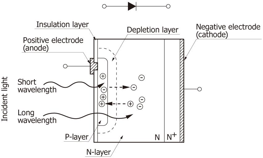
When photons with light energy greater than the band gap are absorbed from the Si photodiode, electrons in the valence band are excited to the conduction band, leaving holes in the valence band.
Figure 2: Silicon photodiodes operating principle
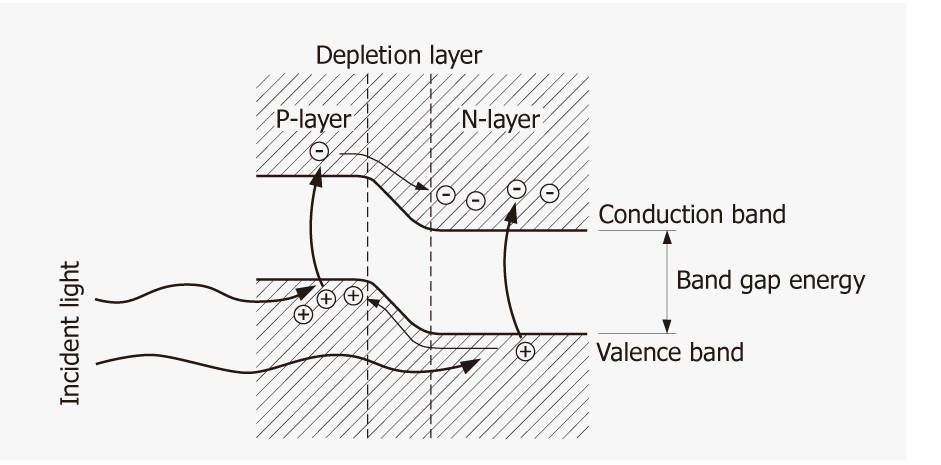
The electric field accelerates these electron-hole pairs from the depletion layer to opposite directions (electrons toward the depletion layer and the holes toward the P-layer). As shown in the figure above, when the incident light has a long wavelength, some electron-hole pairs can be generated in the N-layer. In this case, the electrons are left in the N-layer. The holes are diffused through the N-layer up to the depletion layer, accelerated, and collected in the P-layer. This means that the positive charges are in the P-layer and the negative charges are collected in the N-layer. When the P-layer and the N-layer are connected to an external circuit the electron-hole pairs will flow away and generate a current.
We can explain the behavior of the photodiode with the following circuit diagram:
Figure 3: InGaAs PD circuit example

Il : current generated by incident light (proportional to light level)
Vd : voltage across diode
Id : diode current
Cj : junction capacitance
Rsh : shunt resistance
I’ : shunt resistance current
Rs : series resistance
Vo : output voltage
Io : output current
RL : load resistance [Ω]
Using the above equivalent circuit, the output current (Io) is given by the equation:
Is : photodiode reverse saturation current
q : electron charge
k : Boltzma's constant
T : absolute temperature of photodiode
When Io = 0 we can calculate the open circuit voltage (Voc), expressed by the equation:
If I’ is negligible, since Is increases exponentially with respect to ambient temperature, Voc is inversely proportional to the ambient temperature and proportional to the log of Il. Please consider that this relationship is not maintained when detecting low light levels.
Current vs. voltage characteristics
In dark conditions, the current vs voltage characteristic is the usual, rectifier diode shown as 1 in the following figure. When light strikes the photodiode, the curve at 1 shifts to 2, and the increasing incident light shifts the level to position 3 in parallel.
Figure 4: Rectifier diode behavior
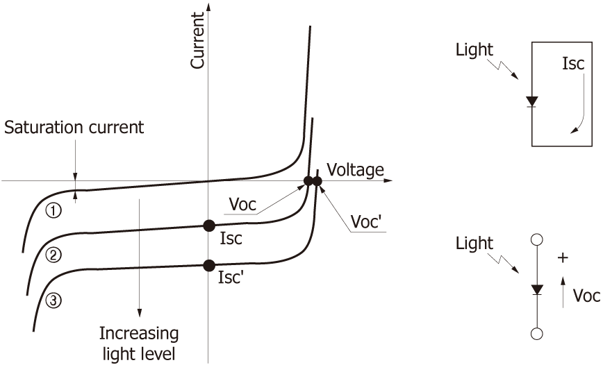
When the light is incident on the Si photodiode, a short circuit current (in this example Isc or Isc’) is generated when the terminals are shorted. This short circuit current is directly proportional to the intensity of the incident light, and it flows from the anode to the cathode. If the circuit is open, an open circuit voltage (Voc or Voc’) will be generated with the positive polarity at the anode.
Linearity characteristics
One of the most important properties of a Si Photodiode is the high level of linearity for the photocurrent with respect to the incident light level:
Figure 5: Photocurrent vs. illuminance (S1223)
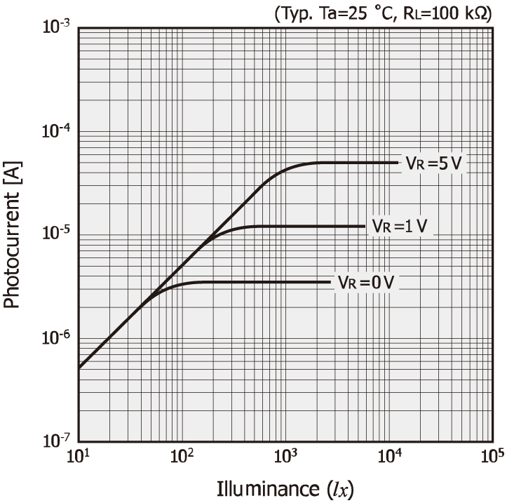
Data based on Hamamatsu Photonics' S1223 SI PIN photodiode.
The lower limit of this linearity is determined by the noise equivalent power, while the upper limit depends on the load resistance and reverse voltage, and is expressed by the following equation:
Psat : input energy [W] at upper limit of linearity (Psat ≤10mW)
Vbi : contact voltage [V] (approx. 0.2 to 0.3V)
Vr : reverse voltage [V]
Rs : photodiode series resistance (several ohms)
RL : load resistance [Ω]
Sλ : photosensitivity [A/W] at wavelenght λ
Please remember that as the series resistance component increases, the linearity degrades.
Noise characteristics
As outlined, the lower limits of light detection for Si photodiodes are determined by their noise characteristics. If we consider the equivalent circuit, Fig 3, the Si photodiode noise current (in) is the sum of the thermal noise current (or Johnson noise current, Ij) of a resistor which approximates the shunt resistance (Rsh) and the shot noise current resulting from the dark current and the photocurrent:
Let’s see how we can describe these three contributions. Ij is viewed as the thermal noise of Rsh and is expressed by this equation:
k : Boltzmann's constant
T : absolute temperature of photodiode
B : noise bandwidth
To describe the short noise ISD we can use the dark current generated from the reverse voltage applied to Si photodiode:
q : electron charge
ID : dark current
The shot noise Isl generated by the photocurrent (Il) due to the incident light and is expressed by the equation.
When Il >> 0.026/Rsh or Il >> Id, the shot noise current Isl becomes predominant compared to the other two dark currents.
A very important characteristic of a Si photodiode is the noise equivalent power (NEP) which is the incident light level required to generate a current equal to the noise current:
In the following figure, we can see a very good match between the data and the theoretical line obtained when Ij is predominant:
Figure 6: NEP vs. shunt resistance (S1226-5BK)
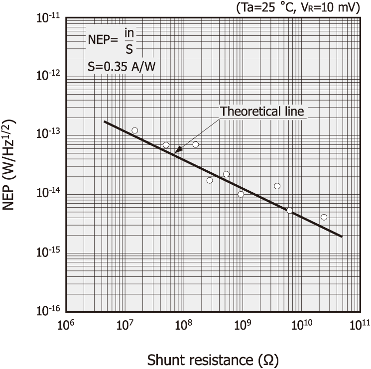
Data based on Hamamatsu Photonics' S1226-5BK Si photodiode.
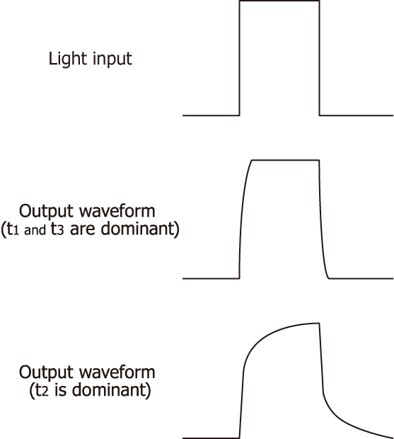
Response speed characteristics
The response speed of a photodiode is a measure of how fast the generated carriers are extracted to an external circuit as output current. The conventional definition for the sensors is the rise time ofthe cut off frequency which is the time required for the output signal to charge from 10% to 90% of the peak output value.
To calculate the rise time we need to consider:
1. Time constant t1 related to terminal capacitance Ct and load resistance Rl
To have a short t1, we need to consider in the design that Ct and Rl are made smaller. Ct is proportional to the photosensitive area (A) and inversely proportional to the depletion layer width (d), and in turn proportional to the electrical resistivity (ƿ) of the substrate material:
It is important to note that applying a reverse voltage also increases dark current. Therefore, it is necessary to be careful, particularly for low-light-level detection.
2. Diffusion time t2 of carriers generated outside the depletion layer
Usually, this time is greater than several microseconds and, in many cases, can be considered negligible.
3. Carrier transit time t3 in the depletion layer
We can describe the transit time in the depletion layer as the ratio between the depletion layer width and the transit speed (vd). The transit speed (vd) is the product between the carrier travelling rate (μ) and the electric field (E) that expresses using the reverse voltage (VR) became (E = VR/D).
We can describe this transit time as:
The total response time will be:
Therefore, the slowest factor becomes predominant. Please consider that t1 and t3 contain factors in conflict, so if we decrease for example t1 we increase t3. During the design phase it is very important to find the right balance between these three factors.
The cutoff frequency (fc) is defined as the frequency at which the photodiode output drops by 3 dB relative to 100% output level, which is maintained while the sine wave frequency is increased. This is roughly approximated from rise time (tr) as:
For applications that require a high-speed response such as optical communications, usually PIN photodiodes are designed such that fewer carriers are generated outside the depletion layer, the terminal capacitance is small and the carrier transit time in the depletion layer is short.
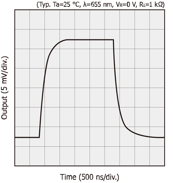
An example of our Si PD:
Figure 7: Examples of response waveforms and frequency characteristics
(a) Response waveforms
(b) Response waveform (S2386-18K)
Hamamatsu Si photodiodes exhibit relatively low dark current when reverse voltage is applied, and have excellent voltage resistance:
Figure 8: Cutoff frequency vs. reverse voltage (S5973, S9055)
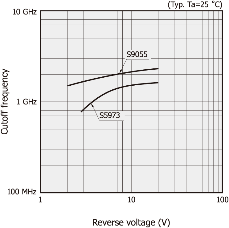
Data based on Hamamatsu Photonics' S5973 and S9055 Si PIN photodiodes.
References
Si Photodiodes, Technical Notes, Hamamatsu Photonics, Oct. 2023: https://www.hamamatsu.com/content/dam/hamamatsu-photonics/sites/documents/99_SALES_LIBRARY/ssd/si_pd_kspd9001e.pdf
- Confirmation
-
It looks like you're in the . If this is not your location, please select the correct region or country below.
You're headed to Hamamatsu Photonics website for GB (English). If you want to view an other country's site, the optimized information will be provided by selecting options below.
In order to use this website comfortably, we use cookies. For cookie details please see our cookie policy.
- Cookie Policy
-
This website or its third-party tools use cookies, which are necessary to its functioning and required to achieve the purposes illustrated in this cookie policy. By closing the cookie warning banner, scrolling the page, clicking a link or continuing to browse otherwise, you agree to the use of cookies.
Hamamatsu uses cookies in order to enhance your experience on our website and ensure that our website functions.
You can visit this page at any time to learn more about cookies, get the most up to date information on how we use cookies and manage your cookie settings. We will not use cookies for any purpose other than the ones stated, but please note that we reserve the right to update our cookies.
1. What are cookies?
For modern websites to work according to visitor’s expectations, they need to collect certain basic information about visitors. To do this, a site will create small text files which are placed on visitor’s devices (computer or mobile) - these files are known as cookies when you access a website. Cookies are used in order to make websites function and work efficiently. Cookies are uniquely assigned to each visitor and can only be read by a web server in the domain that issued the cookie to the visitor. Cookies cannot be used to run programs or deliver viruses to a visitor’s device.
Cookies do various jobs which make the visitor’s experience of the internet much smoother and more interactive. For instance, cookies are used to remember the visitor’s preferences on sites they visit often, to remember language preference and to help navigate between pages more efficiently. Much, though not all, of the data collected is anonymous, though some of it is designed to detect browsing patterns and approximate geographical location to improve the visitor experience.
Certain type of cookies may require the data subject’s consent before storing them on the computer.
2. What are the different types of cookies?
This website uses two types of cookies:
- First party cookies. For our website, the first party cookies are controlled and maintained by Hamamatsu. No other parties have access to these cookies.
- Third party cookies. These cookies are implemented by organizations outside Hamamatsu. We do not have access to the data in these cookies, but we use these cookies to improve the overall website experience.
3. How do we use cookies?
This website uses cookies for following purposes:
- Certain cookies are necessary for our website to function. These are strictly necessary cookies and are required to enable website access, support navigation or provide relevant content. These cookies direct you to the correct region or country, and support security and ecommerce. Strictly necessary cookies also enforce your privacy preferences. Without these strictly necessary cookies, much of our website will not function.
- Analytics cookies are used to track website usage. This data enables us to improve our website usability, performance and website administration. In our analytics cookies, we do not store any personal identifying information.
- Functionality cookies. These are used to recognize you when you return to our website. This enables us to personalize our content for you, greet you by name and remember your preferences (for example, your choice of language or region).
- These cookies record your visit to our website, the pages you have visited and the links you have followed. We will use this information to make our website and the advertising displayed on it more relevant to your interests. We may also share this information with third parties for this purpose.
Cookies help us help you. Through the use of cookies, we learn what is important to our visitors and we develop and enhance website content and functionality to support your experience. Much of our website can be accessed if cookies are disabled, however certain website functions may not work. And, we believe your current and future visits will be enhanced if cookies are enabled.
4. Which cookies do we use?
There are two ways to manage cookie preferences.
- You can set your cookie preferences on your device or in your browser.
- You can set your cookie preferences at the website level.
If you don’t want to receive cookies, you can modify your browser so that it notifies you when cookies are sent to it or you can refuse cookies altogether. You can also delete cookies that have already been set.
If you wish to restrict or block web browser cookies which are set on your device then you can do this through your browser settings; the Help function within your browser should tell you how. Alternatively, you may wish to visit www.aboutcookies.org, which contains comprehensive information on how to do this on a wide variety of desktop browsers.
5. What are Internet tags and how do we use them with cookies?
Occasionally, we may use internet tags (also known as action tags, single-pixel GIFs, clear GIFs, invisible GIFs and 1-by-1 GIFs) at this site and may deploy these tags/cookies through a third-party advertising partner or a web analytical service partner which may be located and store the respective information (including your IP-address) in a foreign country. These tags/cookies are placed on both online advertisements that bring users to this site and on different pages of this site. We use this technology to measure the visitors' responses to our sites and the effectiveness of our advertising campaigns (including how many times a page is opened and which information is consulted) as well as to evaluate your use of this website. The third-party partner or the web analytical service partner may be able to collect data about visitors to our and other sites because of these internet tags/cookies, may compose reports regarding the website’s activity for us and may provide further services which are related to the use of the website and the internet. They may provide such information to other parties if there is a legal requirement that they do so, or if they hire the other parties to process information on their behalf.
If you would like more information about web tags and cookies associated with on-line advertising or to opt-out of third-party collection of this information, please visit the Network Advertising Initiative website http://www.networkadvertising.org.
6. Analytics and Advertisement Cookies
We use third-party cookies (such as Google Analytics) to track visitors on our website, to get reports about how visitors use the website and to inform, optimize and serve ads based on someone's past visits to our website.
You may opt-out of Google Analytics cookies by the websites provided by Google:
https://tools.google.com/dlpage/gaoptout?hl=en
As provided in this Privacy Policy (Article 5), you can learn more about opt-out cookies by the website provided by Network Advertising Initiative:
http://www.networkadvertising.org
We inform you that in such case you will not be able to wholly use all functions of our website.
Close