![]()
Products


We are actively taking measures to improve product quality levels.
Applications


Why Hamamatsu?
Resources


Support


Our company


Investors


United Kingdom (EN)
Select your region or country.
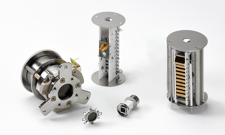
Meeting optical communication demands by revealing the potential of InGaAs photodiodes
The conversion of light into electrical current is made possible by a crucial component – the photodiode. Initially developed using Silicon, these photodiodes facilitated the detection of ultraviolet and visible light. Recent technological advancements have expanded their capabilities to include the detection of infrared light, utilizing materials like Indium Gallium Arsenide for longer wavelengths.
In the rapidly evolving field of telecommunications, the demand for high-data throughput has driven engineers to explore efficient emitters and detectors. This has led to the increased use of light in telecommunications, known as Optical Communication. The benefits include minimal interference, crucial in dense urban areas, and the ability to penetrate physical barriers. Moreover, light enables wireless data transmission over long distances, offering the potential to reduce infrastructure in remote areas. Near-infrared light, with its high frequency, allows faster data transmission and contributes to lower energy consumption in data centers. In this context, we delve into the functionalities of Indium Gallium Arsenide Photodiodes (InGaAs PD), exploring their role in advancing these technological frontiers.
Operating principle
The technical behavior closely resembles that of Silicon photodiodes, with the primary distinction lying in the variance of band gap energy attributable to the different materials employed. The PN junction, constituted by the sensitive surface P-layer and the N-layer, functions as a photoelectric converter. When an InGaAs photodiode (PD) is illuminated with light energy surpassing the band gap energy, electrons in the valence band get elevated to the conduction band, creating holes in the valence band (as illustrated in Figure 1 below).
Figure 1: Silicon photodiodes operating principle
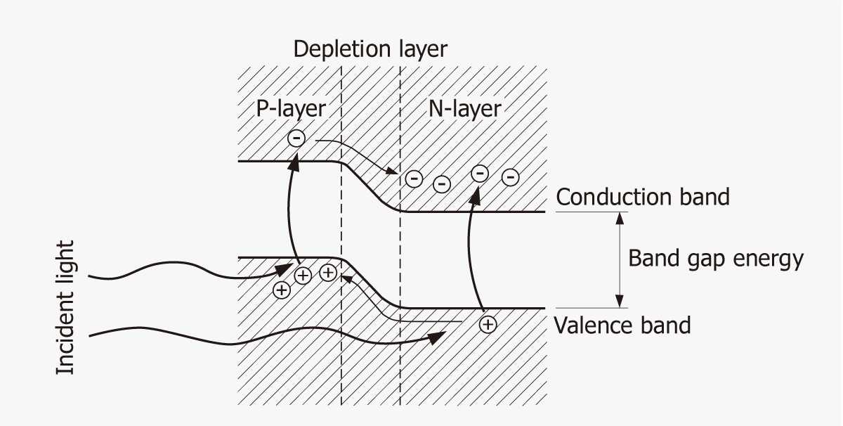
Subsequently, the electric field propels these electron-hole pairs in opposite directions — electrons toward the depletion layer and holes toward the P-layer. Notably, as shown in Figure 1, when incident light has a long wavelength, some electron-hole pairs are generated in the N-layer, resulting in electrons being retained in the N-layer. These holes diffuse through the N-layer to the depletion layer, undergo acceleration, and aggregate in the P-layer. This configuration positions positive charges in the P-layer and negative charges in the N-layer. Connecting the P-layer and N-layer to an external circuit allows the flow of electron-holes, generating a current.
We can summarize the behavior of an InGaAs PD with the following equivalent circuit in Figure 2 below.
Figure 2: InGaAs PD circuit example
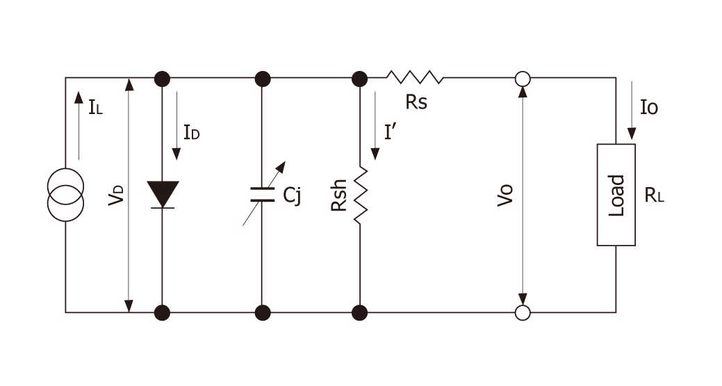
Il : current generated by incident light (proportional to light level)
Vd : voltage across diode
Id : diode current
Cj : junction capacitance
Rsh : shunt resistance
I’ : shunt resistance current
Rs : series resistance
Vo : output voltage
Io : output current
Using the above equivalent circuit, the output current (IO) is given by the equation:
Is : current generated by incident light
(proportional to light level)
q : voltage across diode
k : diode current
T : junction capacitance
Current vs voltage characteristics
In low-light conditions, the current vs voltage characteristics exhibit the typical rectifier diode behavior, as depicted by curve 1 in Figure 3 below. However, when illuminated, the curve shifts to 2, reflecting an increase in incident light. This shift occurs in parallel with position 3.
Figure 3: Rectifier diode behavior
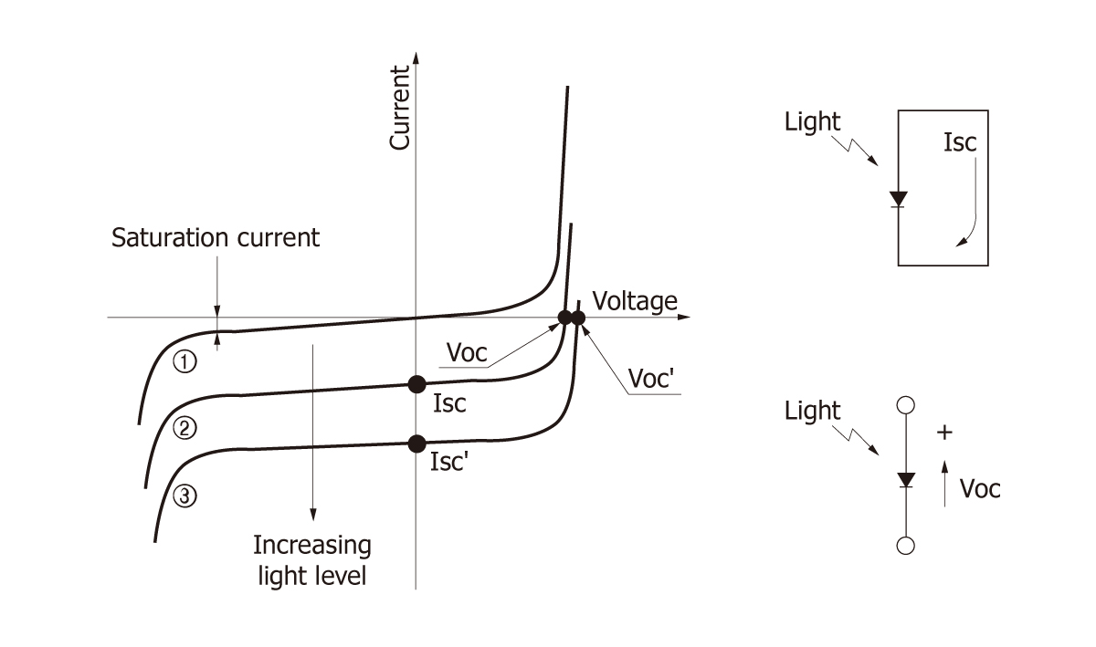
Upon illumination, a short circuit current (Isc or Isc’) proportional to the light level is generated when the InGaAs PD terminals are shorted. Conversely, in an open circuit, an open circuit voltage (Voc or Voc’) is produced, with positive polarity at the anode.
Noise characteristics
The detection sensitivity of InGaAs PDs is constrained by their noise characteristics. Referring back to the equivalent circuit in Figure 3, the InGaAs PD noise current (in) comprises the sum of the thermal noise current (or Johnson noise current, ij) from a resistor approximating the shunt resistance (Rsh), and the shot noise current arising from both dark current and photocurrent as shown in this equation:
Now, let's delve into the descriptions of the three contributions which make up this sum.
1. ij equation
The first is viewed as the thermal noise of Rsh and is given by the following equation:
k : Boltzmann's constant
T : absolute temperature of photodiode
B : noise bandwidth
2. isd equation
To describe the shot noise isD we can use the dark current generated from the reverse voltage applied to the Si photodiode:
q : electron charge
Id : dark current
3. isl equation
The shot noise isL is generated by the photocurrent (IL) due to the incident light expressed by the equation:
When IL is >> 0.026/Rsh or IL >> ID, the shot noise current ISL becomes predominant compared to the other two dark currents.
4. Noise equivalent power
Another important characteristic of photodiodes is their noise equivalent power (NEP) which is the incident light level required to generate a current equal to the noise current:
in : noise current [A/Hz1/2]
S : photosentitivity [A/W]
Spectral response
The cutoff wavelength of photodiodes is expressed by the following equation:
Eg : band gap energy [eV]
For InGaAs PD the band gap energy depends on the composition ratio of In and Ga:
Figure 4: Band gap energy vs composition ratio x of InxGa1-xAs
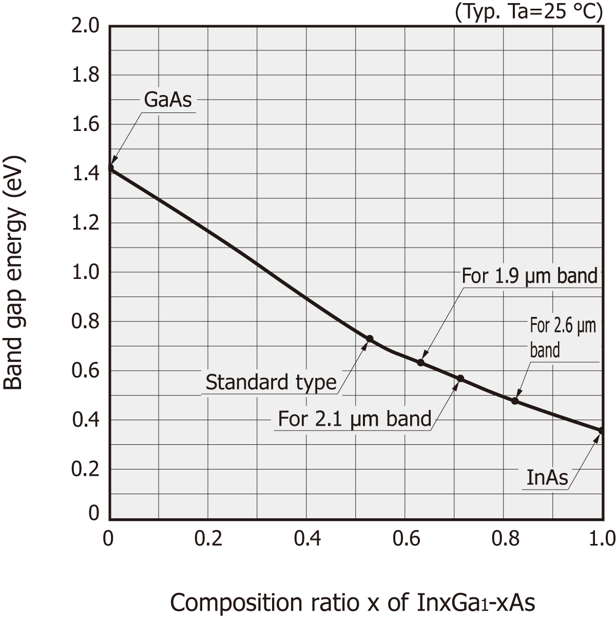
Hamamatsu provides standard types having a cutoff wavelength of 1.7 μm, short-wavelength enhanced types, and long-wavelength types having a cutoff wavelength extending to 1.9 μm, 2.1 μm or up to 2.6 μm.
Response characteristics
The response speed of a photodiode is the measure of how fast the generated carriers are extracted to an external circuit as output current. The conventional definition for the sensors is the rise time of cutoff frequency which is the time required for the output signal to charge from 10% to 90% of the peak output value. We can express the rise time by the following equation:
Ct : terminal capacitance
RL : load resistance
RS : series resistance
Generally, Rs can be disregarded because RL >> Rs. To reduce the rise time, Ct and RL should be lowered, but RL is determined by an external factor and so cannot freely be charged. Ct is proportional to the photosensitive area (A) and is inversely proportional to the square root of the reverse voltage (VR):
Higher response speeds can be obtained by applying a reverse voltage to a photodiode with a small photosensitive area.
Navigating optical advancements with new InGaAs PIN Photodiodes
Hamamatsu Photonics has made speed its priority for the success of optical communication, leading to the development of an ultra-high-speed InGaAs PIN photodiode. This innovation complements their existing 25 Gbps and 50 Gbps photodiodes. Leveraging their optical design and manufacturing expertise, Hamamatsu has incorporated advanced techniques to maximize light guidance into a compact photosensitive area. This approach ensures an equivalent signal-to-noise ratio (S/N ratio) compared to standard products.
The resulting InGaAs PIN photodiode operates effectively at low reverse voltage and demonstrates reliable performance in transmission bands up to 64 Gbps at VR = 2V when paired with an optimized preamp. The culmination of their efforts is exemplified in their latest device, which can be explored further here.
While this represents their most recent achievement, Hamamatsu is committed to pushing boundaries and is actively working towards achieving even higher speeds in their future sensor developments.
Hamamatsu's ongoing commitment to optical innovation
In the realm of optical communication, harnessing the potential of near-infrared light stands out as one of the most pivotal challenges in the coming years. Despite the manifold advantages presented by this light spectrum, it is not without its complexities. Concurrently, engineers worldwide are delving into the exploration of Quantum communications, heralding a new era in secure and efficient data transfer.
With a rich history in the design and production of optical components, Hamamatsu emerges as a reliable partner for those navigating the intricacies of advancing optical communication technologies. Offering a comprehensive suite of products, Hamamatsu is dedicated to supporting customer developments across a diverse array of applications.
Hamamatsu consistently refines products to meet evolving optical communication challenges. Explore our InGaAs photodiodes.
- Confirmation
-
It looks like you're in the . If this is not your location, please select the correct region or country below.
You're headed to Hamamatsu Photonics website for GB (English). If you want to view an other country's site, the optimized information will be provided by selecting options below.
In order to use this website comfortably, we use cookies. For cookie details please see our cookie policy.
- Cookie Policy
-
This website or its third-party tools use cookies, which are necessary to its functioning and required to achieve the purposes illustrated in this cookie policy. By closing the cookie warning banner, scrolling the page, clicking a link or continuing to browse otherwise, you agree to the use of cookies.
Hamamatsu uses cookies in order to enhance your experience on our website and ensure that our website functions.
You can visit this page at any time to learn more about cookies, get the most up to date information on how we use cookies and manage your cookie settings. We will not use cookies for any purpose other than the ones stated, but please note that we reserve the right to update our cookies.
1. What are cookies?
For modern websites to work according to visitor’s expectations, they need to collect certain basic information about visitors. To do this, a site will create small text files which are placed on visitor’s devices (computer or mobile) - these files are known as cookies when you access a website. Cookies are used in order to make websites function and work efficiently. Cookies are uniquely assigned to each visitor and can only be read by a web server in the domain that issued the cookie to the visitor. Cookies cannot be used to run programs or deliver viruses to a visitor’s device.
Cookies do various jobs which make the visitor’s experience of the internet much smoother and more interactive. For instance, cookies are used to remember the visitor’s preferences on sites they visit often, to remember language preference and to help navigate between pages more efficiently. Much, though not all, of the data collected is anonymous, though some of it is designed to detect browsing patterns and approximate geographical location to improve the visitor experience.
Certain type of cookies may require the data subject’s consent before storing them on the computer.
2. What are the different types of cookies?
This website uses two types of cookies:
- First party cookies. For our website, the first party cookies are controlled and maintained by Hamamatsu. No other parties have access to these cookies.
- Third party cookies. These cookies are implemented by organizations outside Hamamatsu. We do not have access to the data in these cookies, but we use these cookies to improve the overall website experience.
3. How do we use cookies?
This website uses cookies for following purposes:
- Certain cookies are necessary for our website to function. These are strictly necessary cookies and are required to enable website access, support navigation or provide relevant content. These cookies direct you to the correct region or country, and support security and ecommerce. Strictly necessary cookies also enforce your privacy preferences. Without these strictly necessary cookies, much of our website will not function.
- Analytics cookies are used to track website usage. This data enables us to improve our website usability, performance and website administration. In our analytics cookies, we do not store any personal identifying information.
- Functionality cookies. These are used to recognize you when you return to our website. This enables us to personalize our content for you, greet you by name and remember your preferences (for example, your choice of language or region).
- These cookies record your visit to our website, the pages you have visited and the links you have followed. We will use this information to make our website and the advertising displayed on it more relevant to your interests. We may also share this information with third parties for this purpose.
Cookies help us help you. Through the use of cookies, we learn what is important to our visitors and we develop and enhance website content and functionality to support your experience. Much of our website can be accessed if cookies are disabled, however certain website functions may not work. And, we believe your current and future visits will be enhanced if cookies are enabled.
4. Which cookies do we use?
There are two ways to manage cookie preferences.
- You can set your cookie preferences on your device or in your browser.
- You can set your cookie preferences at the website level.
If you don’t want to receive cookies, you can modify your browser so that it notifies you when cookies are sent to it or you can refuse cookies altogether. You can also delete cookies that have already been set.
If you wish to restrict or block web browser cookies which are set on your device then you can do this through your browser settings; the Help function within your browser should tell you how. Alternatively, you may wish to visit www.aboutcookies.org, which contains comprehensive information on how to do this on a wide variety of desktop browsers.
5. What are Internet tags and how do we use them with cookies?
Occasionally, we may use internet tags (also known as action tags, single-pixel GIFs, clear GIFs, invisible GIFs and 1-by-1 GIFs) at this site and may deploy these tags/cookies through a third-party advertising partner or a web analytical service partner which may be located and store the respective information (including your IP-address) in a foreign country. These tags/cookies are placed on both online advertisements that bring users to this site and on different pages of this site. We use this technology to measure the visitors' responses to our sites and the effectiveness of our advertising campaigns (including how many times a page is opened and which information is consulted) as well as to evaluate your use of this website. The third-party partner or the web analytical service partner may be able to collect data about visitors to our and other sites because of these internet tags/cookies, may compose reports regarding the website’s activity for us and may provide further services which are related to the use of the website and the internet. They may provide such information to other parties if there is a legal requirement that they do so, or if they hire the other parties to process information on their behalf.
If you would like more information about web tags and cookies associated with on-line advertising or to opt-out of third-party collection of this information, please visit the Network Advertising Initiative website http://www.networkadvertising.org.
6. Analytics and Advertisement Cookies
We use third-party cookies (such as Google Analytics) to track visitors on our website, to get reports about how visitors use the website and to inform, optimize and serve ads based on someone's past visits to our website.
You may opt-out of Google Analytics cookies by the websites provided by Google:
https://tools.google.com/dlpage/gaoptout?hl=en
As provided in this Privacy Policy (Article 5), you can learn more about opt-out cookies by the website provided by Network Advertising Initiative:
http://www.networkadvertising.org
We inform you that in such case you will not be able to wholly use all functions of our website.
Close