![]()
Products


We are actively taking measures to improve product quality levels.
Applications


Why Hamamatsu?
Resources


Support


Our company


Investors


United States (EN)
Select your region or country.
ISTFA 2025
| Event Name | ISTFA 2025 |
|---|---|
| Dates | November 18-19, 2025 |
| Venue | Pasadena Convention Center, Pasadena, CA | Booth 300 |
| Official site | ISTFA 2025 |
At ISTFA 2025, Hamamatsu is proud to showcase our latest innovations for failure analysis systems. Our cutting-edge technologies are designed to elevate your capabilities in semiconductor analysis, empowering you to uncover the root causes of failures with precision and efficiency. Join us at booth 300 to learn how our state-of-the-art equipment and solutions are shaping the future of failure analysis. Discover how Hamamatsu can help you achieve faster, more accurate, and more insightful results. Don't miss this opportunity to explore the next generation of failure analysis systems with Hamamatsu.
Presentations:
Monday, November 17, 2025 | 4:40 PM | Ballroom B | Pasadena Convention Center
Presenters:
Mr. Yunki Jung, Samsung Electronics Co.Ltd, Hwaseong-si, Gyeonggi-do, Korea, Republic of (South)
Mr. Akihito Uchikado, Hamamatsu Photonics K.K., Hamamatsu, Shizuoka, Japan
In this paper, we compare the conventional OBIRCH analysis with the new analysis method Thermo Dynamic Imaging (TDI) to demonstrate the effectiveness of the new method.. We also introduce case studies and provide examples.
Tuesday, November 18, 2025 | 10:50 AM | Ballroom C | Pasadena Convention Center
Presenters:
Mr. Yasushi Oka, Renesas Electronics Corporation, Kodaira, Tokyo, Japan
Mr. Nakaba Matsui, Hamamatsu Photonics K. K, Hamamatsu, Shizuoka, Japan
To improve the success rate of FA, it is important to refine electrical troubleshooting processes. However, EFI techniques face serious challenges with excessive power consumption. This current can disrupt EFI operations. For example, it could cause switching delays due to internal IR drops, leading to unexpected malfunctions in logic operations. Moreover, it may damage the device. To mitigate this issue, minimizing the amount of switching activity during tests is a widely adopted measure to reduce power consumption. However, when the switching activity is reduced, the total test time becomes longer, and so does the looping period for EFI. This weakens every EFI detection signal, causing the 2D location image to be less clear. To address this problem, a PEM with halting at failing logic state was studied, which will not cause excessive switching current. This static PEM method proved effective, offering more accurate localization than conventional dynamic EFI techniques.
Wednesday, November 19, 2025 | Exhibit Hall A&B | Pasadena Convention Center
Presenters:
Dr. Norimichi Chinone, Hamamatsu Corporation, San Jose, CA
Mr. Shota Nozue, Hamamatsu Photonics K.K., Hamamatsu, Shizuoka, Japan
Mr. Shimpei Tominaga, Hamamatsu Photonics K.K., Hamamatsu, Shizuoka, Japan
Mr. Yuhei Aoshima, Hamamatsu Photonics K.K., Hamamatsu, Shizuoka, Japan
Laser-scanning-based thermo-reflectance (TR) was applied to Si device to perform high spatial resolution thermal imaging. The resulting images were mixture of electro-optical and thermal signals, which were separated by means of investigating bias voltage dependency. TR was confirmed to be promising for high spatial resolution thermal imaging on Si devices.
Wednesday, November 19, 2025 | Exhibit Hall A&B | Pasadena Convention Center
Presenters:
Ms. Hyeongki Kim, Samsung Electronics, Hwaseong-si, Gyeonggi-do, Korea, Republic of (South)
Mr. Akihito Uchikado, Hamamatsu Photonics K.K., Hamamatsu, Shizuoka, Japan
Dr. Norimichi Norimichi, Hamamatsu Photonics K.K., Hamamatsu, Shizuoka, Japan
To increase yield and cost competitiveness, FLASH memory device developed vertical stack 3D-VNAND. Furthermore, we introduced Cell over Peripheral (COP), which places peripheral circuits, which were previously located at the same level as memory cells, under the memory cells, thereby reducing the chip size and increasing the number of Dies acquired per wafer. Due to such high stacking and high integration, it is becoming increasingly difficult to identify the location of failures in vertical structures. As one way to solve this problem, we investigated a depth-direction isolation method using lock-in OBIRCH (Optical Beam Induced Resistance Change). As a result, we obtained separate hot spot image results from overlapping memory cells and peripheral circuits. This paper describes these methods and their results.
Wednesday, November 19, 2025 | Exhibit Hall A&B | Pasadena Convention Center
Presenter:
Dr. Norimichi Chinone, Hamamatsu Corporation, San Jose, CA
A data processing algorithm that can break a SNR vs. spatial resolution trade-off in Lock-in OBIRCH was introduced. This algorithm eliminates overlapping among signals caused by significant heat diffusion in low lock-in frequency by deconvoluting heat diffusion. Lock-in OBIRCH data was collected on a test sample followed by data processing, which confirmed the benefit of this algorithm.
Thursday, November 20, 2025 | 9:20 AM | Ballroom C | Pasadena Convention Center
Presenter:
Mrs. Xiangguang Mao, Hamamatsu Photonics K.K, Hamamatsu, Shizuoka, Japan
Electro-optic (EO) probing is a widely used technique in failure analysis (FA). Conventional EO probing techniques use digitizers or oscilloscopes to accumulate data over extended periods to obtain waveforms, making the EO probing method a time-consuming technique for FA. This paper presents a novel approach to using a streak camera in conjunction with Automated Test Equipment (ATE). By adjusting the high reputation test loop over 1 MHz, one can capture the waveform in a short temporal acquisition window with extremely high time resolution.
Featured products:
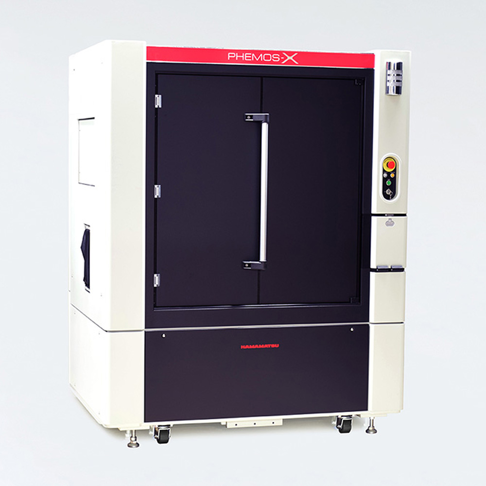
The PHEMOS-X emission microscope C15765-01 is a completely redesigned version of the workhorse PHEMOS-1000. This microscope provides exceptional sensitivity and resolution, allowing you to capture emissions at the finest detail. The laser scanner, optical stage, probe station and macro lens have been redesigned for the advanced semiconductor challenges of the future. Explore the future of microscopy with the PHEMOS-X emission microscope C15765-01.
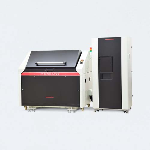
The iPHEMOS-MPX inverted emission microscope C10506-07-06 is your gateway to the world of cutting-edge inverted microscopy, offering unmatched versatility, precision, and imaging capabilities. Its exceptional sensitivity and high-resolution imaging enable you to capture emission signals with unprecedented clarity. Enabling multiple laser, camera and SIL options to be configured on a single system, the iPHEMOS-MPX is the combo system of the future.
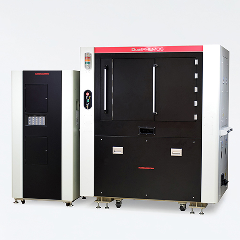
The dual PHEMOS-X emission microscope C16506-01 is a revolutionary breakthrough in electrical failure analysis, featuring both a top side and bottom side microscope in a single system. This allows for wafer analysis from both the front and backside simultaneously to ensure that the fault can be located regardless of its position. Our hope is that this new capability will enable applications that were previously not possible with just a single microscope.
- Confirmation
-
It looks like you're in the . If this is not your location, please select the correct region or country below.
You're headed to Hamamatsu Photonics website for US (English). If you want to view an other country's site, the optimized information will be provided by selecting options below.
In order to use this website comfortably, we use cookies. For cookie details please see our cookie policy.
- Cookie Policy
-
This website or its third-party tools use cookies, which are necessary to its functioning and required to achieve the purposes illustrated in this cookie policy. By closing the cookie warning banner, scrolling the page, clicking a link or continuing to browse otherwise, you agree to the use of cookies.
Hamamatsu uses cookies in order to enhance your experience on our website and ensure that our website functions.
You can visit this page at any time to learn more about cookies, get the most up to date information on how we use cookies and manage your cookie settings. We will not use cookies for any purpose other than the ones stated, but please note that we reserve the right to update our cookies.
1. What are cookies?
For modern websites to work according to visitor’s expectations, they need to collect certain basic information about visitors. To do this, a site will create small text files which are placed on visitor’s devices (computer or mobile) - these files are known as cookies when you access a website. Cookies are used in order to make websites function and work efficiently. Cookies are uniquely assigned to each visitor and can only be read by a web server in the domain that issued the cookie to the visitor. Cookies cannot be used to run programs or deliver viruses to a visitor’s device.
Cookies do various jobs which make the visitor’s experience of the internet much smoother and more interactive. For instance, cookies are used to remember the visitor’s preferences on sites they visit often, to remember language preference and to help navigate between pages more efficiently. Much, though not all, of the data collected is anonymous, though some of it is designed to detect browsing patterns and approximate geographical location to improve the visitor experience.
Certain type of cookies may require the data subject’s consent before storing them on the computer.
2. What are the different types of cookies?
This website uses two types of cookies:
- First party cookies. For our website, the first party cookies are controlled and maintained by Hamamatsu. No other parties have access to these cookies.
- Third party cookies. These cookies are implemented by organizations outside Hamamatsu. We do not have access to the data in these cookies, but we use these cookies to improve the overall website experience.
3. How do we use cookies?
This website uses cookies for following purposes:
- Certain cookies are necessary for our website to function. These are strictly necessary cookies and are required to enable website access, support navigation or provide relevant content. These cookies direct you to the correct region or country, and support security and ecommerce. Strictly necessary cookies also enforce your privacy preferences. Without these strictly necessary cookies, much of our website will not function.
- Analytics cookies are used to track website usage. This data enables us to improve our website usability, performance and website administration. In our analytics cookies, we do not store any personal identifying information.
- Functionality cookies. These are used to recognize you when you return to our website. This enables us to personalize our content for you, greet you by name and remember your preferences (for example, your choice of language or region).
- These cookies record your visit to our website, the pages you have visited and the links you have followed. We will use this information to make our website and the advertising displayed on it more relevant to your interests. We may also share this information with third parties for this purpose.
Cookies help us help you. Through the use of cookies, we learn what is important to our visitors and we develop and enhance website content and functionality to support your experience. Much of our website can be accessed if cookies are disabled, however certain website functions may not work. And, we believe your current and future visits will be enhanced if cookies are enabled.
4. Which cookies do we use?
There are two ways to manage cookie preferences.
- You can set your cookie preferences on your device or in your browser.
- You can set your cookie preferences at the website level.
If you don’t want to receive cookies, you can modify your browser so that it notifies you when cookies are sent to it or you can refuse cookies altogether. You can also delete cookies that have already been set.
If you wish to restrict or block web browser cookies which are set on your device then you can do this through your browser settings; the Help function within your browser should tell you how. Alternatively, you may wish to visit www.aboutcookies.org, which contains comprehensive information on how to do this on a wide variety of desktop browsers.
5. What are Internet tags and how do we use them with cookies?
Occasionally, we may use internet tags (also known as action tags, single-pixel GIFs, clear GIFs, invisible GIFs and 1-by-1 GIFs) at this site and may deploy these tags/cookies through a third-party advertising partner or a web analytical service partner which may be located and store the respective information (including your IP-address) in a foreign country. These tags/cookies are placed on both online advertisements that bring users to this site and on different pages of this site. We use this technology to measure the visitors' responses to our sites and the effectiveness of our advertising campaigns (including how many times a page is opened and which information is consulted) as well as to evaluate your use of this website. The third-party partner or the web analytical service partner may be able to collect data about visitors to our and other sites because of these internet tags/cookies, may compose reports regarding the website’s activity for us and may provide further services which are related to the use of the website and the internet. They may provide such information to other parties if there is a legal requirement that they do so, or if they hire the other parties to process information on their behalf.
If you would like more information about web tags and cookies associated with on-line advertising or to opt-out of third-party collection of this information, please visit the Network Advertising Initiative website http://www.networkadvertising.org.
6. Analytics and Advertisement Cookies
We use third-party cookies (such as Google Analytics) to track visitors on our website, to get reports about how visitors use the website and to inform, optimize and serve ads based on someone's past visits to our website.
You may opt-out of Google Analytics cookies by the websites provided by Google:
https://tools.google.com/dlpage/gaoptout?hl=en
As provided in this Privacy Policy (Article 5), you can learn more about opt-out cookies by the website provided by Network Advertising Initiative:
http://www.networkadvertising.org
We inform you that in such case you will not be able to wholly use all functions of our website.
Close