
Products












We are actively taking measures to improve product quality levels.
Applications





Why Hamamatsu?
Resources



Support


Our company





Investors







United States (EN)
Select your region or country.

Solid Cold Emmi-X camera | Failure analysis system
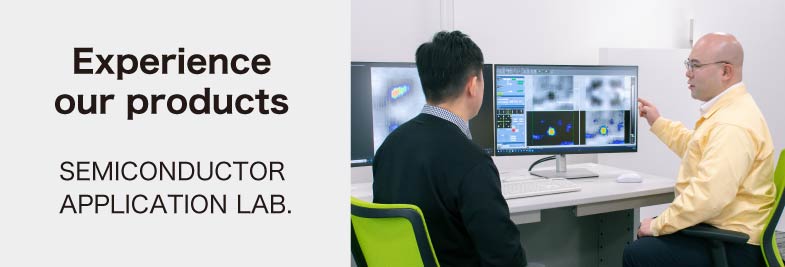
The SEMICONDUCTOR APPLICATION LAB. is a collaborative space designed to foster co-creation with our customers. It offers hands-on demonstrations with actual equipment, including on-site demos with our expert engineers and sample testing prior to purchase.
Solid Cold Emmi-X camera
No LN₂ required — enabling stable 24-hour semiconductor emission analysis
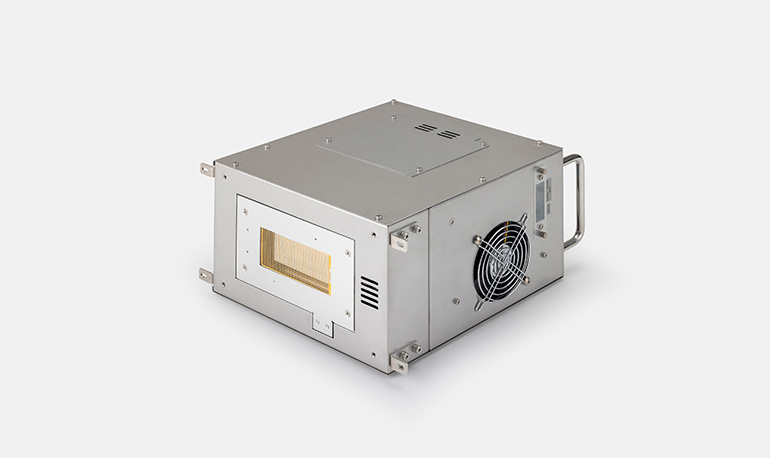
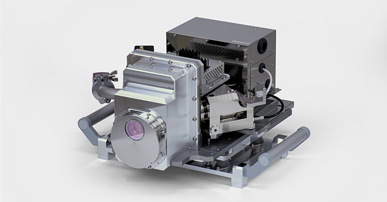
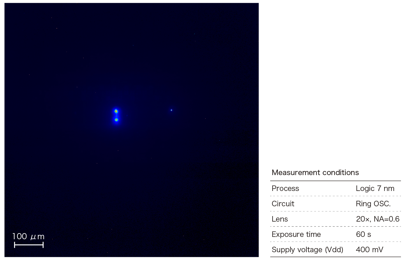
The Solid Cold Emmi-X camera is a photoemission analysis camera featuring Solid Cold cooling, a linear cooling mechanism. It offers higher stability and easier maintenance than LN₂-based systems. It combines a wide field of view with a high S/N sensor and high-speed wavelength switching to enable ultra-low-level emission detection. This allows efficient, high-uptime analysis of advanced logic and high-density memory devices.
Features
Highly stable, low-maintenance cooling system
- High-reliability design with an MTTF of 90 000 hours
- Stable cooling during continuous 24-hour operation
Wide field of view and high S/N for weak emission detection
- Wide field imaging with a 1k × 1k sensor
- Noise reduction enabled by patented technology
High-speed wavelength switching and precise position control
- Wavelength switching in as fast as 5 seconds
- High positional accuracy and stability enabled by a gearless single-axis filter wheel
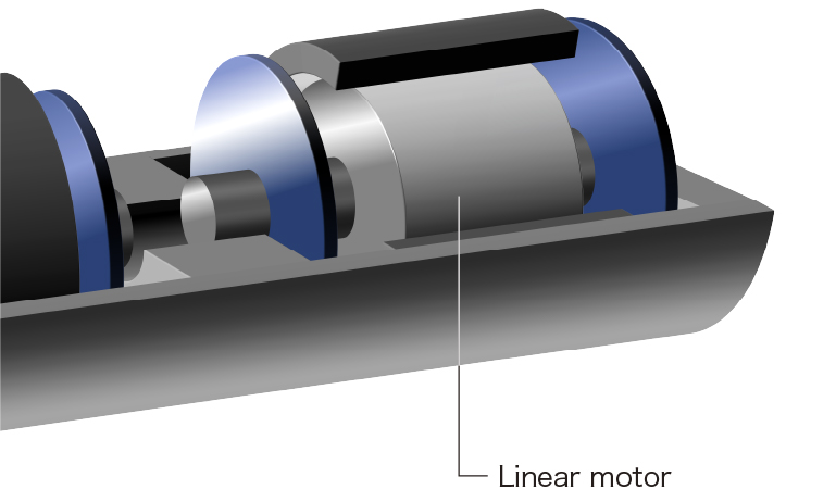
Solid Cold Cooling
- Non-contact motion driven by a linear motor
- Long lifetime (MTTF: 90 000 hours)
Measurement example
Related products
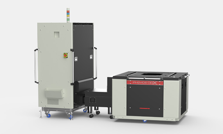
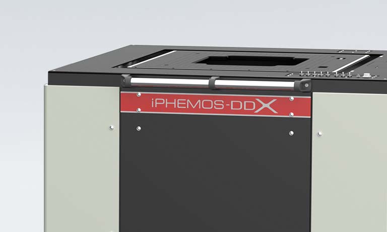
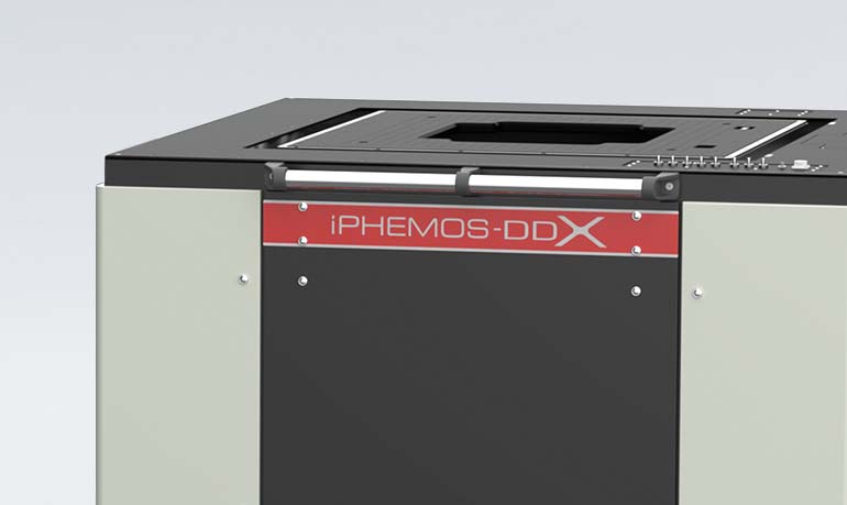
iPHEMOS-DDX is an inverted emission microscope designed for failure analysis of advanced semiconductor packages, including AI chiplets, HBM, 2.5D/3D packages, and large-scale semiconductor packages.
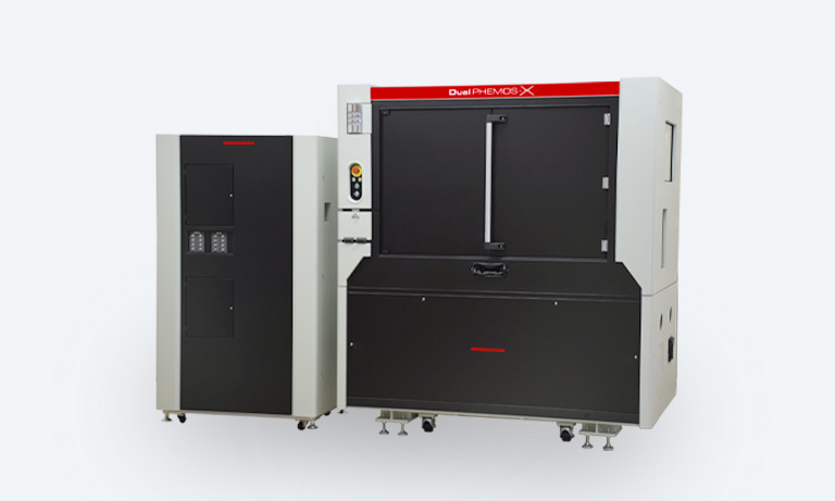
The Dual PHEMOS-X is designed for advanced, 3D, nontransparent devices where simultaneous optical FA may be required from both sides (top and bottom) at the wafer or die level.
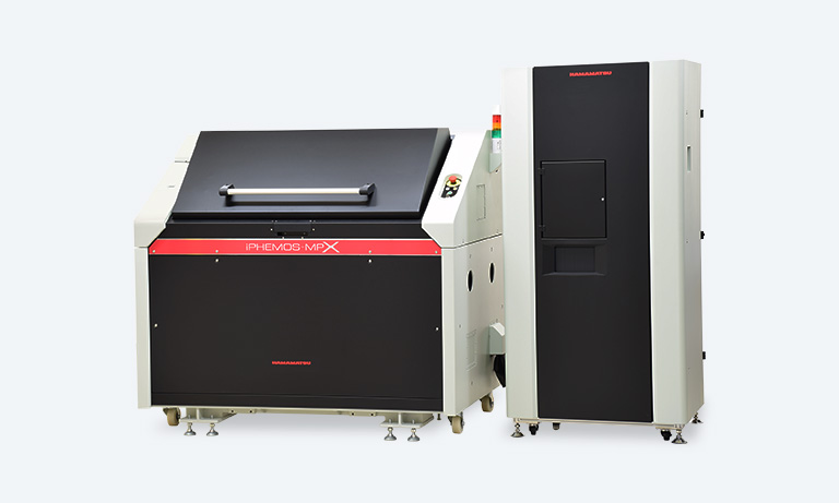
iPHEMOS-MPX is a high-resolution emission microscope that pinpoints failure locations in semiconductor devices by detecting the weak light emissions and heat emissions caused by defects.
SEMICONDUCTOR APPLICATION LAB.
SEMICONDUCTOR APPLICATION LAB. (located in Joko Factory, Hamamatsu City, Shizuoka Prefecture) is a laboratory designed for co-creation with customers. We have equipment to solve your problems, including semiconductor failure analysis and wafer testing.
*It may not work properly depending on your browser and settings.
- Confirmation
-
It looks like you're in the . If this is not your location, please select the correct region or country below.
You're headed to Hamamatsu Photonics website for US (English). If you want to view an other country's site, the optimized information will be provided by selecting options below.
In order to use this website comfortably, we use cookies. For cookie details please see our cookie policy.
- Cookie Policy
-
This website or its third-party tools use cookies, which are necessary to its functioning and required to achieve the purposes illustrated in this cookie policy. By closing the cookie warning banner, scrolling the page, clicking a link or continuing to browse otherwise, you agree to the use of cookies.
Hamamatsu uses cookies in order to enhance your experience on our website and ensure that our website functions.
You can visit this page at any time to learn more about cookies, get the most up to date information on how we use cookies and manage your cookie settings. We will not use cookies for any purpose other than the ones stated, but please note that we reserve the right to update our cookies.
1. What are cookies?
For modern websites to work according to visitor’s expectations, they need to collect certain basic information about visitors. To do this, a site will create small text files which are placed on visitor’s devices (computer or mobile) - these files are known as cookies when you access a website. Cookies are used in order to make websites function and work efficiently. Cookies are uniquely assigned to each visitor and can only be read by a web server in the domain that issued the cookie to the visitor. Cookies cannot be used to run programs or deliver viruses to a visitor’s device.
Cookies do various jobs which make the visitor’s experience of the internet much smoother and more interactive. For instance, cookies are used to remember the visitor’s preferences on sites they visit often, to remember language preference and to help navigate between pages more efficiently. Much, though not all, of the data collected is anonymous, though some of it is designed to detect browsing patterns and approximate geographical location to improve the visitor experience.
Certain type of cookies may require the data subject’s consent before storing them on the computer.
2. What are the different types of cookies?
This website uses two types of cookies:
- First party cookies. For our website, the first party cookies are controlled and maintained by Hamamatsu. No other parties have access to these cookies.
- Third party cookies. These cookies are implemented by organizations outside Hamamatsu. We do not have access to the data in these cookies, but we use these cookies to improve the overall website experience.
3. How do we use cookies?
This website uses cookies for following purposes:
- Certain cookies are necessary for our website to function. These are strictly necessary cookies and are required to enable website access, support navigation or provide relevant content. These cookies direct you to the correct region or country, and support security and ecommerce. Strictly necessary cookies also enforce your privacy preferences. Without these strictly necessary cookies, much of our website will not function.
- Analytics cookies are used to track website usage. This data enables us to improve our website usability, performance and website administration. In our analytics cookies, we do not store any personal identifying information.
- Functionality cookies. These are used to recognize you when you return to our website. This enables us to personalize our content for you, greet you by name and remember your preferences (for example, your choice of language or region).
- These cookies record your visit to our website, the pages you have visited and the links you have followed. We will use this information to make our website and the advertising displayed on it more relevant to your interests. We may also share this information with third parties for this purpose.
Cookies help us help you. Through the use of cookies, we learn what is important to our visitors and we develop and enhance website content and functionality to support your experience. Much of our website can be accessed if cookies are disabled, however certain website functions may not work. And, we believe your current and future visits will be enhanced if cookies are enabled.
4. Which cookies do we use?
There are two ways to manage cookie preferences.
- You can set your cookie preferences on your device or in your browser.
- You can set your cookie preferences at the website level.
If you don’t want to receive cookies, you can modify your browser so that it notifies you when cookies are sent to it or you can refuse cookies altogether. You can also delete cookies that have already been set.
If you wish to restrict or block web browser cookies which are set on your device then you can do this through your browser settings; the Help function within your browser should tell you how. Alternatively, you may wish to visit www.aboutcookies.org, which contains comprehensive information on how to do this on a wide variety of desktop browsers.
5. What are Internet tags and how do we use them with cookies?
Occasionally, we may use internet tags (also known as action tags, single-pixel GIFs, clear GIFs, invisible GIFs and 1-by-1 GIFs) at this site and may deploy these tags/cookies through a third-party advertising partner or a web analytical service partner which may be located and store the respective information (including your IP-address) in a foreign country. These tags/cookies are placed on both online advertisements that bring users to this site and on different pages of this site. We use this technology to measure the visitors' responses to our sites and the effectiveness of our advertising campaigns (including how many times a page is opened and which information is consulted) as well as to evaluate your use of this website. The third-party partner or the web analytical service partner may be able to collect data about visitors to our and other sites because of these internet tags/cookies, may compose reports regarding the website’s activity for us and may provide further services which are related to the use of the website and the internet. They may provide such information to other parties if there is a legal requirement that they do so, or if they hire the other parties to process information on their behalf.
If you would like more information about web tags and cookies associated with on-line advertising or to opt-out of third-party collection of this information, please visit the Network Advertising Initiative website http://www.networkadvertising.org.
6. Analytics and Advertisement Cookies
We use third-party cookies (such as Google Analytics) to track visitors on our website, to get reports about how visitors use the website and to inform, optimize and serve ads based on someone's past visits to our website.
You may opt-out of Google Analytics cookies by the websites provided by Google:
https://tools.google.com/dlpage/gaoptout?hl=en
As provided in this Privacy Policy (Article 5), you can learn more about opt-out cookies by the website provided by Network Advertising Initiative:
http://www.networkadvertising.org
We inform you that in such case you will not be able to wholly use all functions of our website.
Close