![]()
Products


We are actively taking measures to improve product quality levels.
Applications


Why Hamamatsu?
Resources


Support


Our company


Investors


United Kingdom (EN)
Select your region or country.
Industrial Tomography
Detecting hidden defects with microfocus X-ray CT
Industrial manufacturers increasingly rely on computed tomography (CT) for non-destructive testing of batteries, plastics, composite materials, and semiconductor devices. This approach allows the complex internal structures of these materials to be inspected for hidden defects – such as micro-voids, cracks, or inclusions – without damaging components. The X-ray source plays a critical role in CT system design [1], with microfocus X-ray sources enabling high-resolution inspection by minimizing geometric blur and operating across a voltage range suitable for both 2D and 3D non-destructive testing.
The challenge: achieving high-resolution inspection in practice
The growing number of applications for industrial CT systems is driving demand for higher resolution and greater imaging flexibility, creating a number of challenges for system designers needing to balance several competing performance requirements. The size of the X-ray source focal spot is a major limitation, as focal spots in the millimeter range can provide higher output power, but introduce geometric blur, making it difficult to resolve fine features. Microfocus X-ray sources effectively minimize blur and enhance image detail, with the trade-off of lower tube currents thatcan extend acquisition time [1].
These performance requirements must be addressed at the system level, particularly in how the X-ray source is integrated. Open type sources can deliver higher voltages and output powers for demanding inspection tasks, supporting high-performance applications, while sealed type sources offer a compact, lowmaintenance alternative that simplifies integration into industrial CT systems and enables reliable long-term operation. If the source has a monoblock structure, the design also eliminates the need for high-voltage cables. Achieving this balance between focal spot size, output power, and system integration remains a central challenge in the development of industrial CT systems [2, 3].
Advanced microfocus X-ray sources
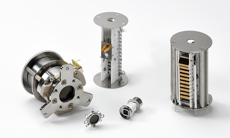
To address these challenges, Hamamatsu Photonics has eveloped a complete range of microfocus X-ray sources for high-resolution industrial CT inspection including both open and sealed type microfocus X-ray sources. These components combine small focal spot sizes with high X-ray tube voltages of up to 300 kV (180 kV for sealed types), enabling the detection of fine internal features while maintaining the penetration required for a wide range of materials and component types.
In particular, sealed-type microfocus X-ray sources are well suited to the inspection of batteries, plastics, composites, and semiconductor devices, where both resolution and reliability are critical. Their compact designs simplify integration and reduce the need for additional infrastructure, supporting stable, lowmaintenance operation. They also support both 2D and 3D non-destructive testing, allowing engineers to adapt inspection workflows to different application needs, from offline inspection analysis to integration into production workflows [2].
The range includes microfocus X-ray sources based on transmission-type designs [4] also referred to as targetground (TGND) technology. In this configuration, a thin target is positioned immediately adjacent to the X-ray exit window inside the tube. This allows the effective X-ray focal spot to be located very close to the external surface, enabling the object to be placed closer to the focal spot. As a result, the focus-to-object distance is reduced, leading to higher geometric magnification and improved ability to resolve extremely fine features.
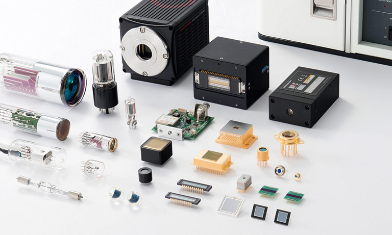
Hamamatsu Photonics also offers a range of detectors for CT applications, including flat panel detectors. This is particularly important for high-resolution imaging, where the performance of the X-ray source must be matched by detector capability to fully resolve fine internal features.
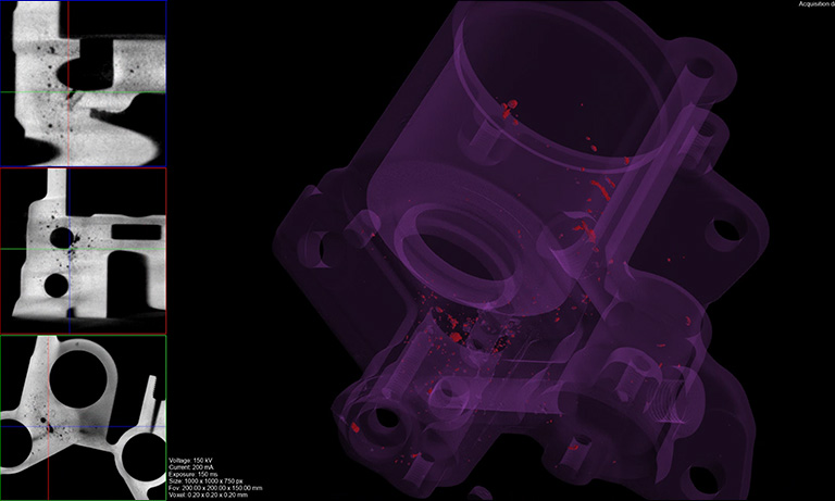
Integration into industrial microfocus X-ray CT systems
Industrial CT platforms are typically supplied as complete inspection systems combining X-ray sources, detectors, motion stages, and reconstruction software, but cost and system complexity have traditionally limited uptake. One European CT system developer set out to address this issue by creating a more compact, flexible, and convenient platform capable of being widely deployed – including closer to production lines – to enable routine inspection of small components.
In this system, the component for inspection is placed on a rotating stage inside the scanning chamber, then the X-ray source and detector capture a series of projection images as the object rotates. These projections are then reconstructed to generate a 3D representation of the component.
The company chose a sealed type microfocus X-ray source from Hamamatsu Photonics for integration into its compact CT platform, helping to achieve:
- Improved image resolution, enabling detection of very small internal defects
- Higher reliability, thanks to stable and consistent X-ray output
- Multi-material inspection, allowing analysis of plastic, rubber, and metal components
- Compact system design, simplifying integration into space-constrained industrial environments
Application highlights
The images below illustrate representative CT inspection results across a range of materials and applications, demonstrating the system’s ability to resolve fine internal features and analyze complex structures non-destructively.
Automotive parts inspection
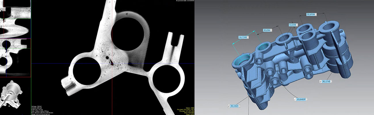
Cross-sectional CT image of an object composed of a porous region, a denser region, and a metallic part, which appears as the brightest area in the image. Courtesy of MDA S.r.l.
Composite materials with sharp surface structures
Cross-sectional CT image of an object composed of a porous region, a denser region, and a metallic part, which appears as the brightest area in the image. Courtesy of MDA S.r.l.
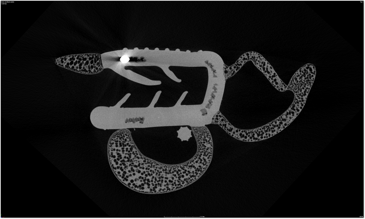
Deformable rubber items
CT image of two rubber gaskets, demonstrating non-destructive inspection and metrology without cutting or deforming the component. Courtesy of MDA S.r.l.
The future of CT imaging in non-destructive testing
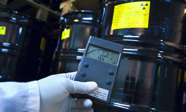
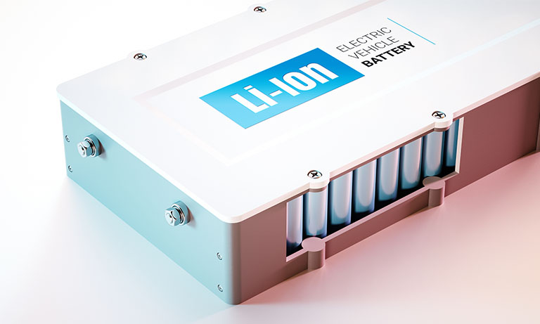
Demand for industrial CT inspection is expected to grow as components become more complex and manufacturing tolerances tighten. This is driving two key directions in system development: higher spatial resolution for applications such as desktop CT and semiconductor inspection, and higher X-ray energies and output powers to enable inspection of larger or denser components. For example, increasing battery capacity is leading to larger and more complex lithium-ion battery structures, requiring higher X-ray energies for effective inspection. In parallel, there is a growing push to deploy CT systems closer to production lines, enabling faster inspection and reducing reliance on off-site analyses. Meeting these requirements depends on continued advances in X-ray source and detector technologies, as well as their integration into compact, reliable inspection systems.
Developments in microfocus X-ray source design are helping to support both higher resolution and improved penetration, enabling CT systems to address an increasingly wide range of industrial applications. Hamamatsu Photonics’ development roadmap is designed to keep pace with the key trends shaping industrial CT. The company is actively advancing microfocus X-ray sources and complementary imaging technologies to address these evolving requirements, while also supporting their integration into complete CT systems. Through this approach, Hamamatsu works closely with system integrators as a technology partner, supporting the development of next-generation industrial CT platforms.
References
[1] L. De Chiffre, “Industrial applications of computed tomography,” CIRP Annals, vol. 63, no. 2, pp. 655-677, 2014. doi: 10.1016/j.cirp.2014.05.011.
[2] Hamamatsu Photonics, MFX | Microfocus X-ray Sources Catalog. [Online]. Available: https://www.hamamatsu.com/content/dam/hamamatsu-photonics/sites/documents/99_SALES_LIBRARY/etd/MFX_TXPR1041E.pdf
[3] A. Hirakimoto, “Microfocus X-ray computed tomography and its industrial applications,” Analytical Sciences, vol. 17, pp. i123-i125, 2001. [Online]. Available: https://www.jstage.jst.go.jp/article/analscisp/17icas/0/17icas_0_i123/_pdf/-char/en
[4] Hamamatsu Photonics, Microfocus X-ray source L15851. [Online]. Available: https://www.hamamatsu.com/eu/en/product/light-and-radiation-sources/microfocus-x-ray-source/L15851.html
- Confirmation
-
It looks like you're in the . If this is not your location, please select the correct region or country below.
You're headed to Hamamatsu Photonics website for GB (English). If you want to view an other country's site, the optimized information will be provided by selecting options below.
In order to use this website comfortably, we use cookies. For cookie details please see our cookie policy.
- Cookie Policy
-
This website or its third-party tools use cookies, which are necessary to its functioning and required to achieve the purposes illustrated in this cookie policy. By closing the cookie warning banner, scrolling the page, clicking a link or continuing to browse otherwise, you agree to the use of cookies.
Hamamatsu uses cookies in order to enhance your experience on our website and ensure that our website functions.
You can visit this page at any time to learn more about cookies, get the most up to date information on how we use cookies and manage your cookie settings. We will not use cookies for any purpose other than the ones stated, but please note that we reserve the right to update our cookies.
1. What are cookies?
For modern websites to work according to visitor’s expectations, they need to collect certain basic information about visitors. To do this, a site will create small text files which are placed on visitor’s devices (computer or mobile) - these files are known as cookies when you access a website. Cookies are used in order to make websites function and work efficiently. Cookies are uniquely assigned to each visitor and can only be read by a web server in the domain that issued the cookie to the visitor. Cookies cannot be used to run programs or deliver viruses to a visitor’s device.
Cookies do various jobs which make the visitor’s experience of the internet much smoother and more interactive. For instance, cookies are used to remember the visitor’s preferences on sites they visit often, to remember language preference and to help navigate between pages more efficiently. Much, though not all, of the data collected is anonymous, though some of it is designed to detect browsing patterns and approximate geographical location to improve the visitor experience.
Certain type of cookies may require the data subject’s consent before storing them on the computer.
2. What are the different types of cookies?
This website uses two types of cookies:
- First party cookies. For our website, the first party cookies are controlled and maintained by Hamamatsu. No other parties have access to these cookies.
- Third party cookies. These cookies are implemented by organizations outside Hamamatsu. We do not have access to the data in these cookies, but we use these cookies to improve the overall website experience.
3. How do we use cookies?
This website uses cookies for following purposes:
- Certain cookies are necessary for our website to function. These are strictly necessary cookies and are required to enable website access, support navigation or provide relevant content. These cookies direct you to the correct region or country, and support security and ecommerce. Strictly necessary cookies also enforce your privacy preferences. Without these strictly necessary cookies, much of our website will not function.
- Analytics cookies are used to track website usage. This data enables us to improve our website usability, performance and website administration. In our analytics cookies, we do not store any personal identifying information.
- Functionality cookies. These are used to recognize you when you return to our website. This enables us to personalize our content for you, greet you by name and remember your preferences (for example, your choice of language or region).
- These cookies record your visit to our website, the pages you have visited and the links you have followed. We will use this information to make our website and the advertising displayed on it more relevant to your interests. We may also share this information with third parties for this purpose.
Cookies help us help you. Through the use of cookies, we learn what is important to our visitors and we develop and enhance website content and functionality to support your experience. Much of our website can be accessed if cookies are disabled, however certain website functions may not work. And, we believe your current and future visits will be enhanced if cookies are enabled.
4. Which cookies do we use?
There are two ways to manage cookie preferences.
- You can set your cookie preferences on your device or in your browser.
- You can set your cookie preferences at the website level.
If you don’t want to receive cookies, you can modify your browser so that it notifies you when cookies are sent to it or you can refuse cookies altogether. You can also delete cookies that have already been set.
If you wish to restrict or block web browser cookies which are set on your device then you can do this through your browser settings; the Help function within your browser should tell you how. Alternatively, you may wish to visit www.aboutcookies.org, which contains comprehensive information on how to do this on a wide variety of desktop browsers.
5. What are Internet tags and how do we use them with cookies?
Occasionally, we may use internet tags (also known as action tags, single-pixel GIFs, clear GIFs, invisible GIFs and 1-by-1 GIFs) at this site and may deploy these tags/cookies through a third-party advertising partner or a web analytical service partner which may be located and store the respective information (including your IP-address) in a foreign country. These tags/cookies are placed on both online advertisements that bring users to this site and on different pages of this site. We use this technology to measure the visitors' responses to our sites and the effectiveness of our advertising campaigns (including how many times a page is opened and which information is consulted) as well as to evaluate your use of this website. The third-party partner or the web analytical service partner may be able to collect data about visitors to our and other sites because of these internet tags/cookies, may compose reports regarding the website’s activity for us and may provide further services which are related to the use of the website and the internet. They may provide such information to other parties if there is a legal requirement that they do so, or if they hire the other parties to process information on their behalf.
If you would like more information about web tags and cookies associated with on-line advertising or to opt-out of third-party collection of this information, please visit the Network Advertising Initiative website http://www.networkadvertising.org.
6. Analytics and Advertisement Cookies
We use third-party cookies (such as Google Analytics) to track visitors on our website, to get reports about how visitors use the website and to inform, optimize and serve ads based on someone's past visits to our website.
You may opt-out of Google Analytics cookies by the websites provided by Google:
https://tools.google.com/dlpage/gaoptout?hl=en
As provided in this Privacy Policy (Article 5), you can learn more about opt-out cookies by the website provided by Network Advertising Initiative:
http://www.networkadvertising.org
We inform you that in such case you will not be able to wholly use all functions of our website.
Close