![]()
Products


We are actively taking measures to improve product quality levels.
Applications


Why Hamamatsu?
Resources


Support


Our company


Investors


United Kingdom (EN)
Select your region or country.
iPMSEL
Overview
We have developed a chip-size light source which can emit arbitrary beam patterns by controlling the spatial phase of the light. We named this device iPMSEL® (integrable Phase Modulating Surface Emitting Lasers, US trademark Reg. No. 5410112).
Recently, LiDAR technology has been attracting much attention in various fields such as collision prevention, surveying, and 3D measurement. LiDAR requires a light source that can scan beam patterns. For this purpose, a suitable light source should satisfy several conditions: small size, lack of mechanical moving structures, electrical control of beam patterns, etc. The size and weight of the light source are particularly important for drones, because the weight and available space in drones are severely limited (see Fig. 1). Small beam-scanning light sources have application possibilities in other fields such as capsule endoscopy (Fig. 2) and natural 3D displays (Fig. 3).
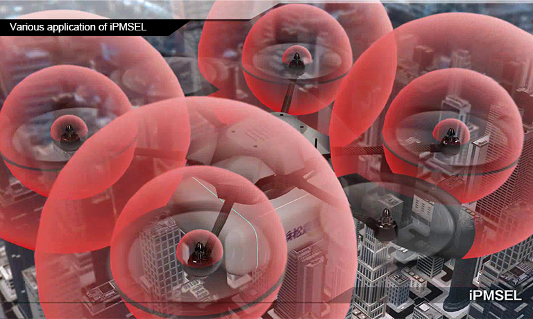
Fig. 1 Application of iPMSEL 1 (LiDAR for drone)
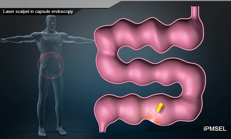
Fig. 2 Application of iPMSEL 1 (LiDAR for drone)
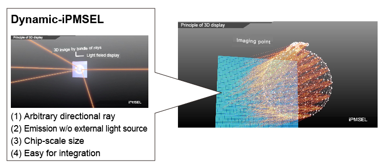
Fig. 3 Application of iPMSEL 3 (3D display)
Static-iPMSELs
We have successfully demonstrated a Static-iPMSEL device which emits static arbitrary beam patterns. As shown in Fig. 4, it can emit designated arbitrary beam patterns from a needle-size chip. Even though the beam pattern is static, the potential applications of this technology include 3D measurement and indication such as head-up display. As an example of 3D measurement, we can measure a 3D shape by projecting beam patterns such as multi dot, fringe, and mesh patterns onto the object, then taking pictures, and calculating the position from the distortion of the projecting beam patterns (see Fig. 5, left). If the light source is miniaturized into a needle-size chip, a portable 3D measurement system can also be possible (see Fig. 5, right). We also demonstrated large-scale multi-dot beam patterns of more than 10,000 points which is useful to 3D measurement (see Fig. 6). 3D measurement systems are in high demand for facial recognition and 3D modeling in mobile phones. We therefore believe that Static-iPMSEL can be used for these purposes.
In addition to developing the Static-iPMSEL and Arrayed-iPMSEL devices, in which static beam patterns are projected or switched, we are also developing a Dynamic-iPMSEL device, in which arbitrary beam patterns are emitted and controlled dynamically from a chip.
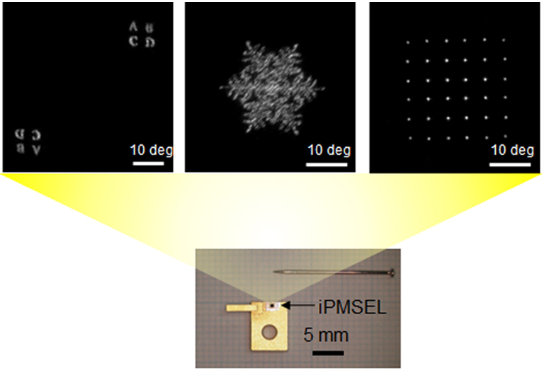
Fig. 4 Far field patterns of Static-iPMSELs
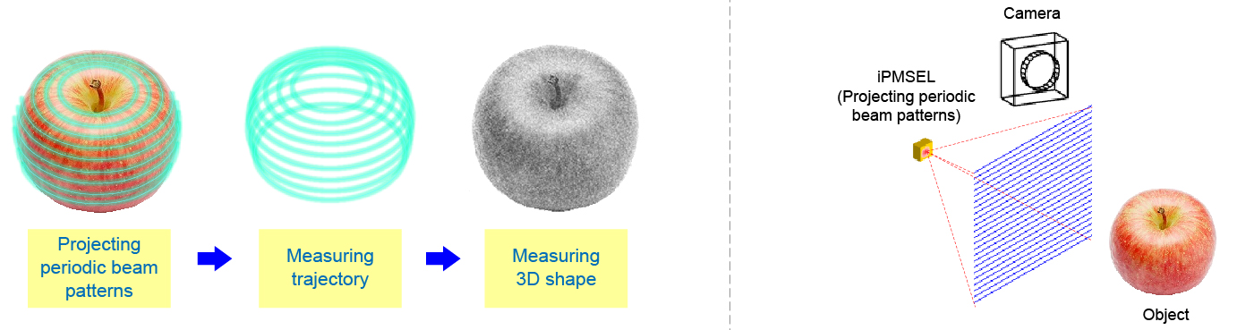
Fig. 5 Principle of 3D measurement
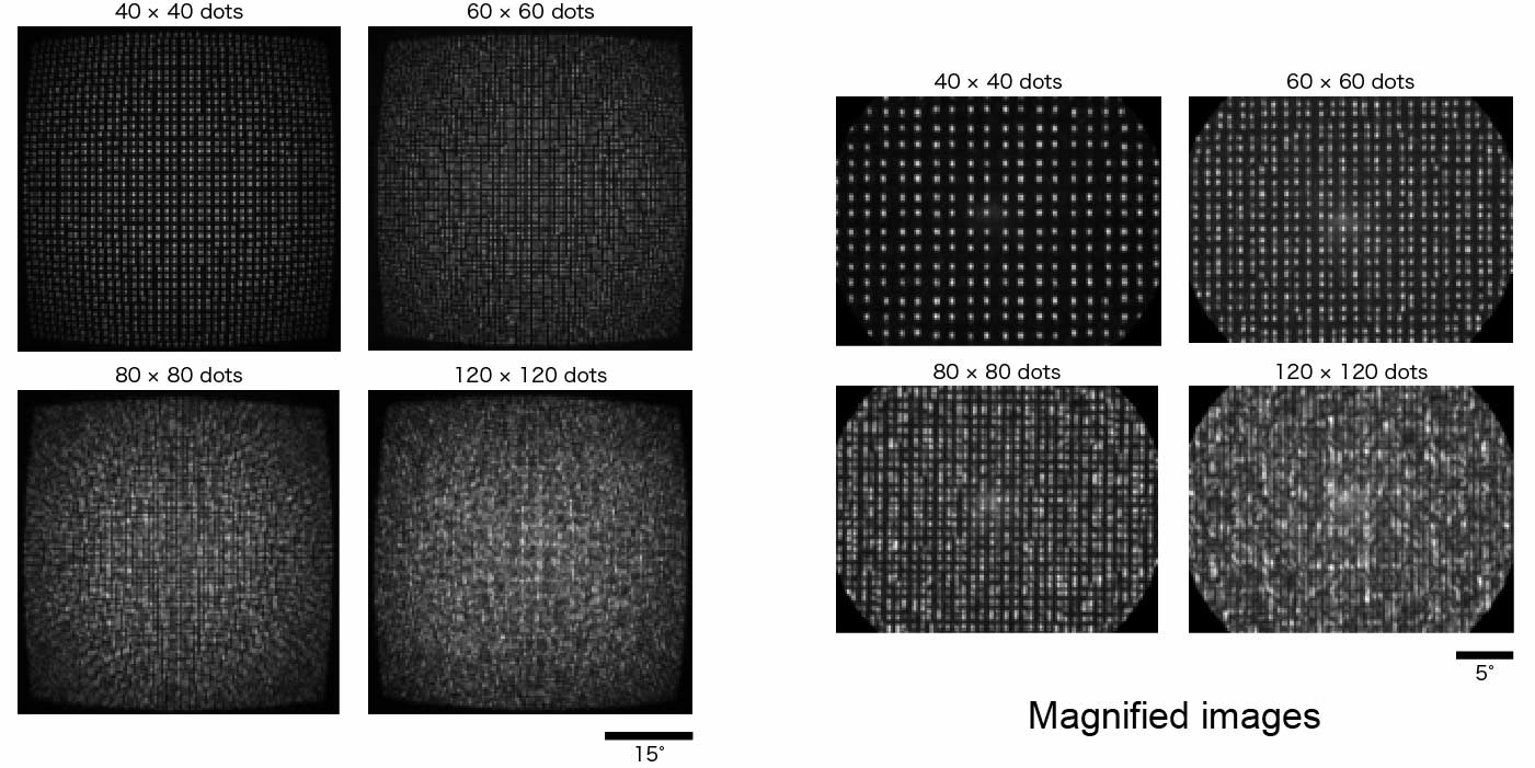
Fig. 6 Large-scale multi-dot beam patterns of Static-iPMSELs
Features of Static-iPMSELs
The schematics of static-iPMSELs compared with those of the conventional technique (a combination of DOEs and VCSELs) are shown in Fig. 7.
Because the size of the static-iPMSELs is one order of magnitude smaller, two orders of denser integration are feasible, enabling us to switch between numbers of patterns that are two orders of magnitude larger than those of the conventional technique from the same area. Note that the beam divergence increases due to the small size. Meanwhile, vertical spot noise beams are not shown in the static-iPMSELs, and we believe that they are suitable for dense integration.
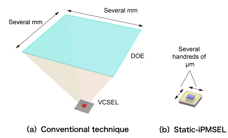
Fig. 7 Schematics of 2D pattern light source
*DOE: Diffractive optical element, VCSEL: Vertical cavity surface emitting laser
Operation of the Arrayed-iPMSELs
Topic①:Pattern switching from monolithic array
Monolithic array is easily achieved by integrating several devices into same wafer by using planer process.
It enables pattern switching with highly accurate positional alignment that is required in highly accurate 3D measurement.
Related press release:Hamamatsu Photonics has succeeded in creating an iPMSEL array that emits light beams in switchable patterns(26. Oct. 2021)
Fig. 8 Pattern switching from monolithic array
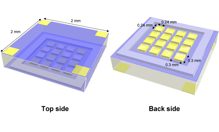
Fig. 9 Schematic of monolithic array
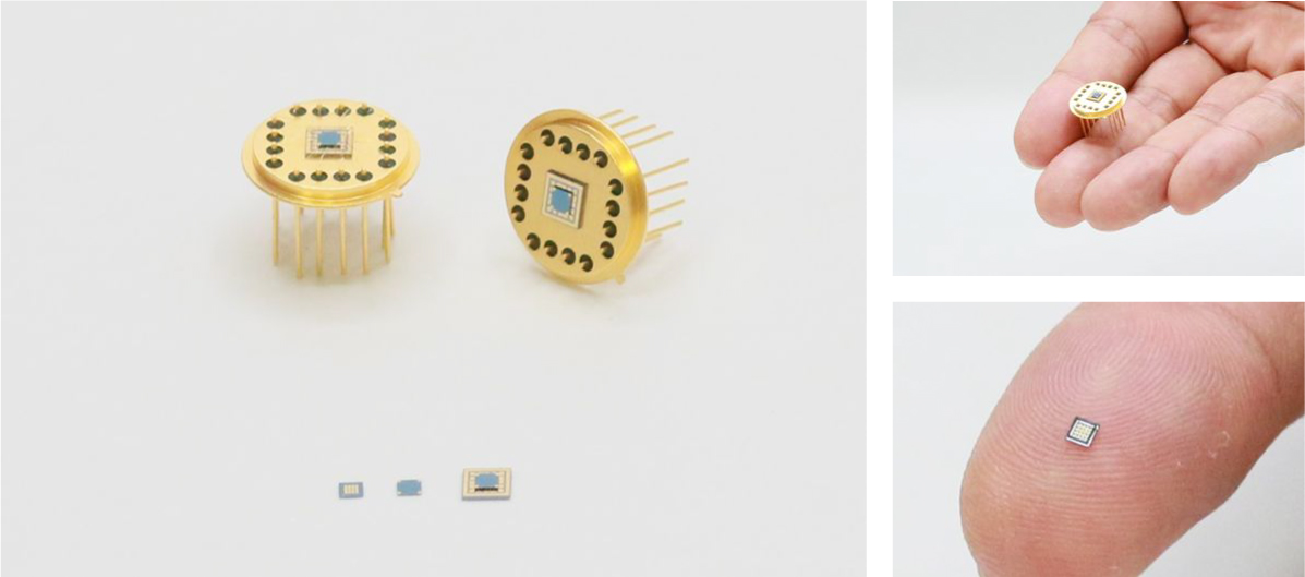
Fig. 10 Picture of the monolithic array (bonded on TO-8 base)
Highly accurate 3D measurement is achieved by switching the fringe projection as shown in Fig. 11.
Fig.12 indicated the phase distribution from the fringe patterns. By using triangulation,the phase is converted into the 3D positional information.
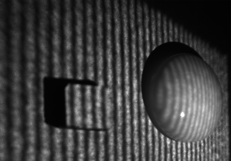
Fig. 11 Switching of fringe projections
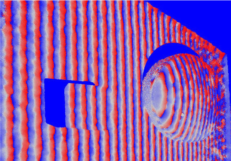
Fig. 12 3D measurement (phase measurement)
Topic②:Direct focusing (1)
Direct focusing from on-chip size surface emitting lasers is achieved by using appropriate holographic design.
Following example shows focusing with sufficiently short focal length of about 300 µm. We successfully achieved narrow focusing with focusing diameter of 6.0 µm which corresponds to double of the diffraction limit.
See ref. [7] for the details.
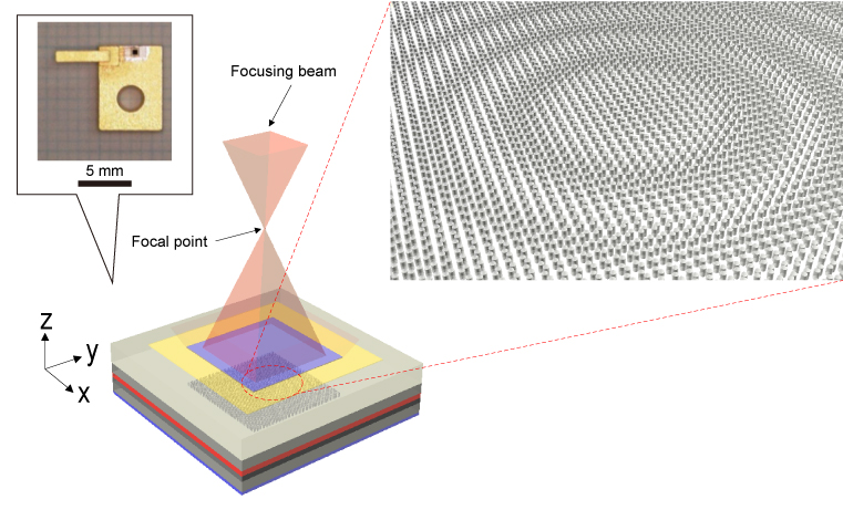
Fig. 13 Schematic of the hole arrangement
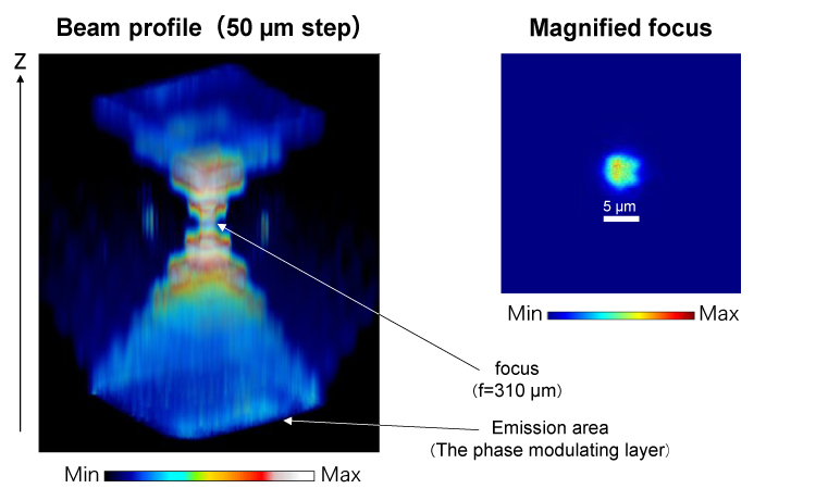
Fig. 14 Beam profile and magnified focus
Topic③:Direct focusing (2)
It is also possible to focus multiple point with multiple focal length at same time.
See ref. [9] for the details.
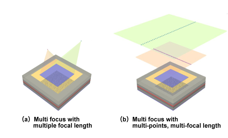
Fig. 15 Example of multi focus
Topic④:Direct focusing (3)
The other application of direct focusing of the iPMSEL is projection of low-noise fringe patterns which is desired in highly accurate 3D measurement. Ordinary holographic fringe pattern causes speckle-like noise that comes from Interference between neighboring dot patterns in far field. To avoid the interference, 1D line dot patterns with sufficient spacing is extended by using 1D focusing in the orthogonal direction. As the result, the low-noise fringe pattern is realized as shown below which is quite useful for the 3D measurement.
See ref. [8] for the details.
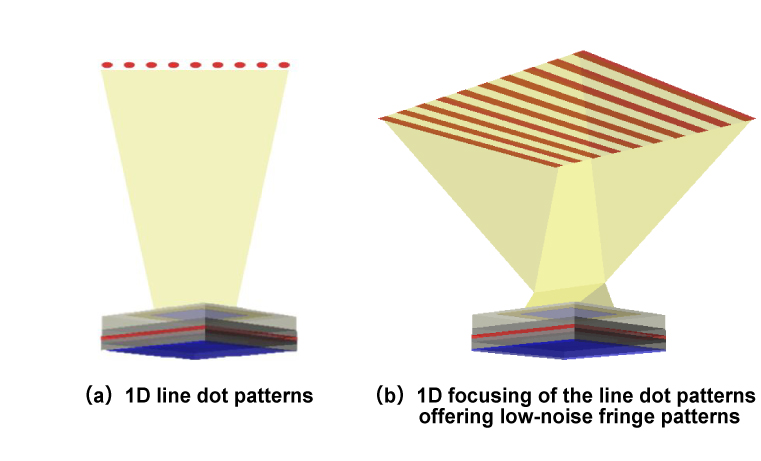
Fig. 16 Example of beam pattern irradiation
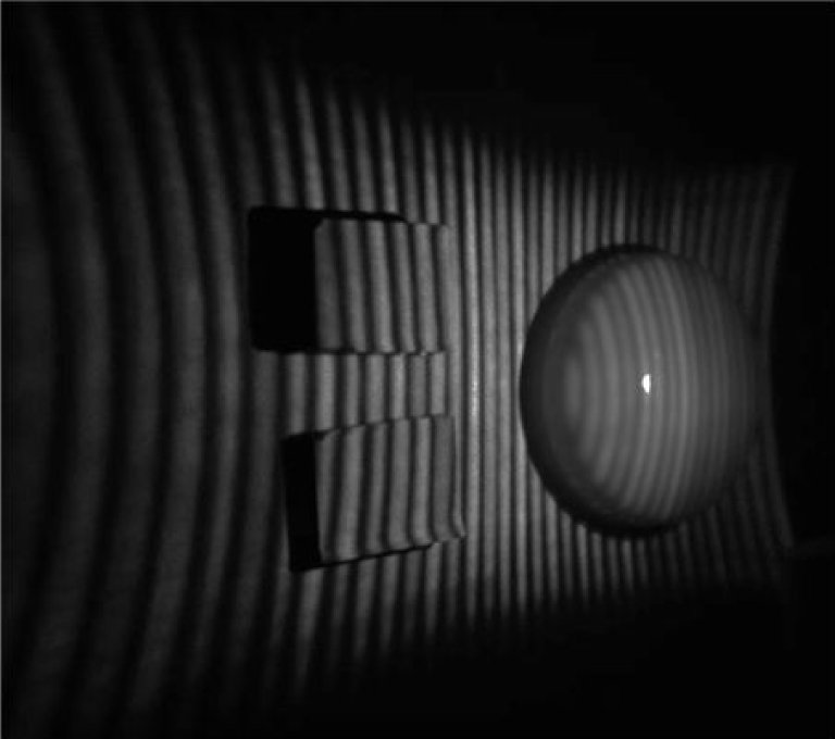
Fig. 17 Projection of 1D focusing fringe pattern
Future applications
■Natural 3D display
The rays emitted from 3D objects can be reproduced by the pixel arrays which can control the beam pattern arbitrary. This type of mechanism is widely utilized in a “light-field display”. For this purpose, the Dynamic-iPMSEL can be used as the pixel of 3D display in the future. When a natural 3D display is developed and widely spread, it will offer a possibility for a vivid communication between family members and friends who live at a distance from each other, becoming a new indispensable communication tool.
■LiDAR
Recently, LiDAR technology is applied in collision prevention of automobiles, surveying, and 3D measurement. Ordinary LiDAR systems are equipped with mechanical beam-scanning units which make the system size large. Development of a chip-size electrical beam-scanning system without mechanical moving structures will lead to a significant reduction of the system’s size and weight. A light source of this kind will be a key device in drones, for example, where the total weight and available space are limited. We believe that iPMSEL will be perfect for such applications.
■Laser scalpel in capsule endoscopy
Medical examination involving endoscopy can be particularly painful. However, a capsule endoscope can mitigate the insertion pain during diagnostic examination. In fact, simultaneous diagnosis and treatment of the affected part in vivo will be possible if the capsule endoscope will be equipped with a laser scalpel which can control beam patterns arbitrary. We think that iPMSEL can be used for this purpose in the future.
■3D measurement
3D shape can be measured by the following simple procedure. Projecting beam patterns such as multi dot, fringe, and mesh patterns onto the object and taking pictures, then calculating the 3D shape from the distortion of the beam pattern. So far, we succeeded to emit such beam patterns from Static-iPMSEL device which emits static arbitrary beam patterns.
■Indication
Static-iPMSEL device emits characters or even gray scale beam patterns, as shown in Fig. 4. Moreover, the beam patterns can be switched from the chip-scale device, as shown in the video of Arrayed-iPMSEL. Therefore, we think that they can be applied in small head-up displays where the number of beam patterns is limited, or in a chip-scale indicating device which indicates a variety of marks.
Detailed description of the device
In this section, we describe the structure and the operating principle of the Static-iPMSEL. Schematics of the device is shown in Fig. 8. Similar to an ordinary semiconductor laser, the Static-iPMSEL consists of the cladding layers, which confine carriers (electrons and holes) between them, and the active layer, where light is generated by radiative recombination on substrates. In contrast to the ordinary laser diode, the novel phase-modulating layer, where sub µm-scale holes are arranged, is formed near the active layer. Then, what does this layer act as? As shown in the top-view SEM image of the phase-modulating layer in Fig. 8, there are holes which seem to be arranged periodically at first glance. However, the holes are slightly shifted from the periodic lattice point of a square lattice. In fact, the centers of gravity of the holes are rotationally shifted on the circle whose center corresponds to the lattice point O of the square lattice. According to the target beam patterns, the positional shift of each hole is determined by using computer-generated hologram technique.
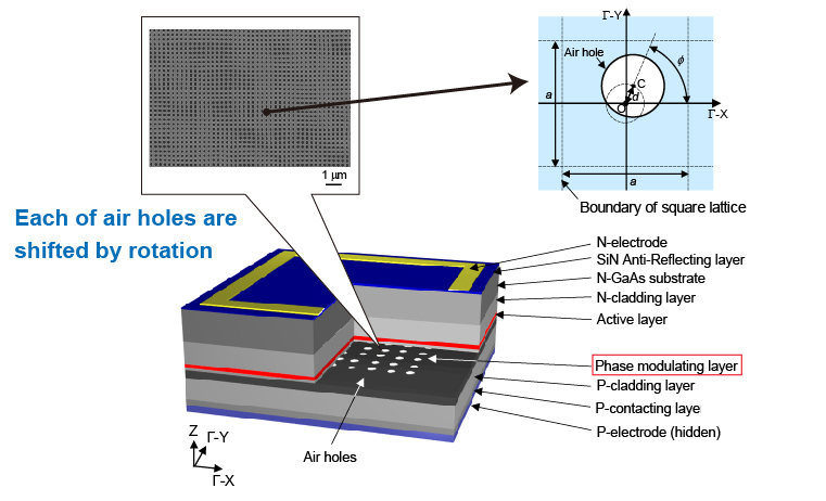
Fig. 18 Structure of iPMSELs
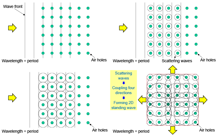
Fig. 19 Principle of in-plane resonance in iPMSELs
When currents are injected into the device, the light waves are generated at the active layer due to the radiative recombination and emitted in various directions. Parts of these light waves are coupled to the phase-modulating layers near the active layer.
Then what happens in the phase-modulating layer? Here, we consider a periodic hole array (2D photonic crystal) for simplicity, because the shift of the holes is small and negligible. When the light wave from left side incident to the periodic holes as shown in fig. 9, the light wave is scattered spherically at each hole. Note that the waves scattering from each hole interfere constructively in four directions in Fig. 9 (namely, up, down, left, and right) because the period of the holes corresponds to the wavelength, which results in a 2π-phase shift of the scattering waves at each hole in four directions. This is called “diffraction” in physics. When these four diffracted light waves propagate, they are also diffracted to the same four directions, coupled with each other, and spread over the entire in-plane region. Note that coupling of counter-propagating waves creates standing waves which do not propagate in any direction and oscillate at a stationary position. Therefore, 2D standing waves are formed in the phase-modulating layers. The phase-modulating layer acts as a resonance cavity of the laser because of the standing waves. (“Formation of 2D standing wave”.)
When the period of the hole equals the light wavelength as shown in Fig. 20(a), four in-plane diffracted waves are also diffracted in vertical directions, and plane waves are emitted in vertical directions. Since the plane waves are emitted from a broad area that expands to several hundreds of micrometer, it gives rise to a narrow spot beam whose beam divergence angle is less than 1º.
Next, we explain intuitively what happens in the phase-modulating layers where holes are shifted from periodic arrangement. Since the positional shift of the holes is small, 2D standing waves are still formed while the output beam patterns are changed. Fig. 20(b) shows the schematics of the output beam patterns diffracted from the phase-modulating layer. Due to the positional shift of the holes from the periodic position, the vertically diffracted waves proceed/retard locally, so that the wave front is spatially modulated (“spatial modulation of beam patterns”). Based on our matured skills in holography, we can easily design the “spatial phase modulation” for the arbitrary target beam patterns. In summary, the phase-modulating layer forms “2D standing waves” that act as a resonance cavity of the laser and a “spatial phase modulation” of the output beam patterns at the same time. Thus, the Static-iPMSEL device can emit arbitrary beam patterns from a needle-tip size chip.
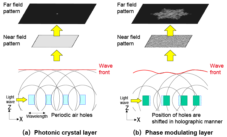
Fig. 20 Principle of phase modulation in iPMSELs
Reference
- Y. Kurosaka, et al., “Phase-modulating lasers toward on-chip integration,” Scientific Reports 6, 30138 (2016).
- Y. Takiguchi, et al., “Principle of beam generation in on-chip 2D beam pattern projecting lasers,” Optics Express 26, 10787-10800 (2018).
- K. Hirose, et al., “Removal of surface-normal spot beam from on-chip 2D beam pattern projecting lasers,” Optics Express 26, 29854-29866 (2018).
- Y. Kurosaka, et al., "Beam Pattern Projecting On-Chip Lasers at Visible Wavelength," CLEO 2019, SM4N.2, (2019).
- K. Hirose, et al., “200×200 µm2 structured light source,” Optics Express 28, 37307-37321 (2020).
- Y. Kurosaka, et al., “Replication of band structure in an arbitrary wave vector by holographic modulation,” Physical Review B 103, 245310 (2021).
- K. Hirose, et al., “Direct-focusing surface-emitting laser,” Optics Express 30, 3066-3075 (2022).
- K. Hirose, et al., “On-chip size, low-noise fringe pattern projector offering highly accurate 3D measurement,” Optics Letters 48, 1387-1390 (2023).
- K. Hirose, et. al., "Multi-focusing surface-emitting lasers," Optics Express 31, 17137-17147 (2023).
*References 1-9 (except 4) are open access.
- Confirmation
-
It looks like you're in the . If this is not your location, please select the correct region or country below.
You're headed to Hamamatsu Photonics website for GB (English). If you want to view an other country's site, the optimized information will be provided by selecting options below.
In order to use this website comfortably, we use cookies. For cookie details please see our cookie policy.
- Cookie Policy
-
This website or its third-party tools use cookies, which are necessary to its functioning and required to achieve the purposes illustrated in this cookie policy. By closing the cookie warning banner, scrolling the page, clicking a link or continuing to browse otherwise, you agree to the use of cookies.
Hamamatsu uses cookies in order to enhance your experience on our website and ensure that our website functions.
You can visit this page at any time to learn more about cookies, get the most up to date information on how we use cookies and manage your cookie settings. We will not use cookies for any purpose other than the ones stated, but please note that we reserve the right to update our cookies.
1. What are cookies?
For modern websites to work according to visitor’s expectations, they need to collect certain basic information about visitors. To do this, a site will create small text files which are placed on visitor’s devices (computer or mobile) - these files are known as cookies when you access a website. Cookies are used in order to make websites function and work efficiently. Cookies are uniquely assigned to each visitor and can only be read by a web server in the domain that issued the cookie to the visitor. Cookies cannot be used to run programs or deliver viruses to a visitor’s device.
Cookies do various jobs which make the visitor’s experience of the internet much smoother and more interactive. For instance, cookies are used to remember the visitor’s preferences on sites they visit often, to remember language preference and to help navigate between pages more efficiently. Much, though not all, of the data collected is anonymous, though some of it is designed to detect browsing patterns and approximate geographical location to improve the visitor experience.
Certain type of cookies may require the data subject’s consent before storing them on the computer.
2. What are the different types of cookies?
This website uses two types of cookies:
- First party cookies. For our website, the first party cookies are controlled and maintained by Hamamatsu. No other parties have access to these cookies.
- Third party cookies. These cookies are implemented by organizations outside Hamamatsu. We do not have access to the data in these cookies, but we use these cookies to improve the overall website experience.
3. How do we use cookies?
This website uses cookies for following purposes:
- Certain cookies are necessary for our website to function. These are strictly necessary cookies and are required to enable website access, support navigation or provide relevant content. These cookies direct you to the correct region or country, and support security and ecommerce. Strictly necessary cookies also enforce your privacy preferences. Without these strictly necessary cookies, much of our website will not function.
- Analytics cookies are used to track website usage. This data enables us to improve our website usability, performance and website administration. In our analytics cookies, we do not store any personal identifying information.
- Functionality cookies. These are used to recognize you when you return to our website. This enables us to personalize our content for you, greet you by name and remember your preferences (for example, your choice of language or region).
- These cookies record your visit to our website, the pages you have visited and the links you have followed. We will use this information to make our website and the advertising displayed on it more relevant to your interests. We may also share this information with third parties for this purpose.
Cookies help us help you. Through the use of cookies, we learn what is important to our visitors and we develop and enhance website content and functionality to support your experience. Much of our website can be accessed if cookies are disabled, however certain website functions may not work. And, we believe your current and future visits will be enhanced if cookies are enabled.
4. Which cookies do we use?
There are two ways to manage cookie preferences.
- You can set your cookie preferences on your device or in your browser.
- You can set your cookie preferences at the website level.
If you don’t want to receive cookies, you can modify your browser so that it notifies you when cookies are sent to it or you can refuse cookies altogether. You can also delete cookies that have already been set.
If you wish to restrict or block web browser cookies which are set on your device then you can do this through your browser settings; the Help function within your browser should tell you how. Alternatively, you may wish to visit www.aboutcookies.org, which contains comprehensive information on how to do this on a wide variety of desktop browsers.
5. What are Internet tags and how do we use them with cookies?
Occasionally, we may use internet tags (also known as action tags, single-pixel GIFs, clear GIFs, invisible GIFs and 1-by-1 GIFs) at this site and may deploy these tags/cookies through a third-party advertising partner or a web analytical service partner which may be located and store the respective information (including your IP-address) in a foreign country. These tags/cookies are placed on both online advertisements that bring users to this site and on different pages of this site. We use this technology to measure the visitors' responses to our sites and the effectiveness of our advertising campaigns (including how many times a page is opened and which information is consulted) as well as to evaluate your use of this website. The third-party partner or the web analytical service partner may be able to collect data about visitors to our and other sites because of these internet tags/cookies, may compose reports regarding the website’s activity for us and may provide further services which are related to the use of the website and the internet. They may provide such information to other parties if there is a legal requirement that they do so, or if they hire the other parties to process information on their behalf.
If you would like more information about web tags and cookies associated with on-line advertising or to opt-out of third-party collection of this information, please visit the Network Advertising Initiative website http://www.networkadvertising.org.
6. Analytics and Advertisement Cookies
We use third-party cookies (such as Google Analytics) to track visitors on our website, to get reports about how visitors use the website and to inform, optimize and serve ads based on someone's past visits to our website.
You may opt-out of Google Analytics cookies by the websites provided by Google:
https://tools.google.com/dlpage/gaoptout?hl=en
As provided in this Privacy Policy (Article 5), you can learn more about opt-out cookies by the website provided by Network Advertising Initiative:
http://www.networkadvertising.org
We inform you that in such case you will not be able to wholly use all functions of our website.
Close